
Tips & Tricks: Avoiding Solder Escape/Wick during Reflow
on
Have you ever wondered why sometimes you have poor Solder joints on your PCB’s!
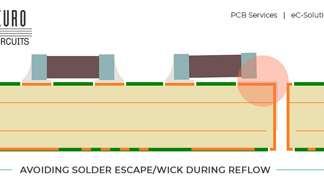
One of the main reasons is that the Solder Paste flows away from the pad on the PCB during Reflow, this is known as Solder Escape, Solder Wick or Solder Drainage.
Why does this happen, well there are a few reasons but inevitably they are all the result of Thermal Dissipation during the Reflow process. Basically, the heat flows away from the pad on the PCB to a larger Thermal conductive area that’s connected to the pad and unprotected by a Soldermask Dam, these include:
- Via Holes
- Copper Areas
- Larger Tracks
Below is an example (animation) of a Via Hole that is too close to a SM pad and therefore has no Soldermask Dam to stop the Solder Paste escaping into the hole.

There are several solutions to this issue and Eurocircuits is developing a PCB Assembly Guideline to help Designers understand and creating PCB layouts that may create potential Assembly issues.
Please visit our PCB Assembly Guidelines section on Solder Escape/Wick for more information on how to avoid this issue.
Should you have any questions about any of our services, please feel free to get in touch via email, telephone or instantly with our online chat  during office hours. We will be more than happy to help.
Discussion (0 comments)