
VLSI Symposia: Samsung use EUV for 7 nm process
July 12, 2018
on
on
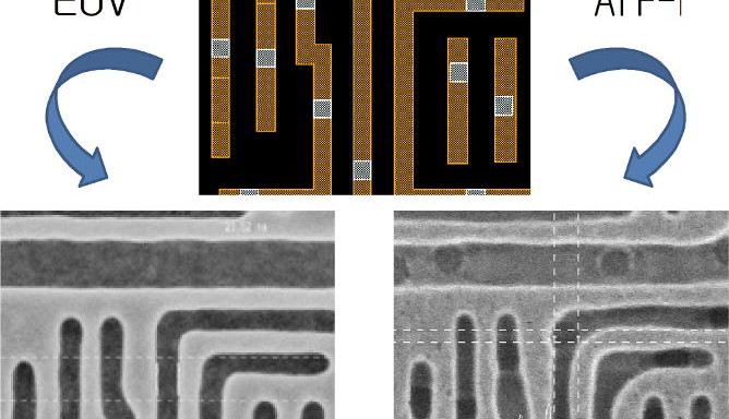
Samsung unveiled its upcoming 7nm FinFET technology at the VLSI Symposia recently. Samsung is expected to be the first of the major semiconductor manufacturers to employ Extreme Ultra Violet (EUV) lithography for the process – EUV provides improved pattern uniformity and lower manufacturing costs compared to standard extreme-scaling multi-patterning processes.
Samsung uses EUV with additional front-end scaling, special designs, and a single diffusion layer to produce the smallest FinFET transistors with a fin pitch of 27 and gate pitch 54 nm. Power consumption is reduced to around 50 to 60% of current 10 nm technology.
Samsung has also produced a 256 Mb SRAM array with a cell size of only 0.0262 μm² along with CPU / GPU logic circuits that conform to NBTI reliability requirements.
They have also developed a low-power 8nm FinFET logic process specifically for mobile, high performance and low power applications. This new 8LPP process is a scaled down version of the existing 10nm volume production process, by comparison it uses 7% less power, is around 15% smaller and is able to operate at just 0.35 V.
Read full article
Hide full article
Discussion (0 comments)