
PCB by CNC (Part 1): How To Mill Your PCB Tracks Instead Of Etching Them
on
For prototyping or very small-volume production purposes, the use of external PCB services may become expensive or, to the very least, turn out to be a time-consuming route. For different reasons, the chemical etching may also be discarded. In these cases, CNC-milling of a printed circuit could be considered as a valid alternative for accuracy, ease of implementation and, most importantly, for giving a very fast way to have your beloved board finished and ready for soldering!
Anyone involved in practical electronics, whether for pleasure or work, sooner or later "runs into" the need to make a circuit board. Prototyping is done with breadboards or multi-hole matrix PCBs, but these are almost always circuits that are difficult to consider definitive, although some people manage to craft well-done designs with these media. The high road of the prototype, which can also become final, is that of the PCB (Printed Circuit Board), which is usually made by a professional service, with costs that nowadays are more or less within the reach of every pocket. But that of the service is an option for a final circuit, which has passed all the tests and perhaps needs to go into production, even for small runs. However, if you are in the design phase, and experimentation requires a stable circuit with a ground plane, and you expect to make changes after testing, then the cost of a professional PCB may not be worth it.
Until a very few years ago, the only way to make a homemade PCB was to fix the circuit design onto a copper plate, by photo-etching or toner transfer, and then dip the plate in ferric chloride (or other suitable chemicals) to remove excess copper; but while a circuit in SMT (Surface Mount Technology) was ready at that point, if we are talking about THT (Through Hole Technology) the second step to be dealt with was that of drilling, and here the problems began because, as we all know, the holes are not all the same size and therefore require different diameter drill bits, not to mention the need to center each hole precisely; it is clear that this step represented a considerable waste of time, with results that were rarely perfect. These techniques are still used today because the steps up to etching in ferric chloride are quick and give good results, but dealing with chemicals in small environments, such as a room at home or a small laboratory, can be very dangerous.
The advent of CNCs, now widely available due to their increasingly affordable cost, has certainly revolutionized the world of prototyping, making it possible to make technically perfect circuits, without having to handle chemicals and, most importantly, obtaining correctly sized and perfectly centered holes. In these new articles, we will use this excellent combination, along with a variety of open-source or free software, to learn how to make an average PCB with PTH components; we will then see all the steps necessary to obtain the file that will drive the CNC for both the etching and drilling phases. In addition, we will propose a simple mechanical addition that will allow the board to be machined to be attached to the holding plate with great ease and precision.
The programs we used are: Eagle 9.6.2 free, to generate the Gerber files, FlatCAM v.8.5 open source, downloadable from here, that will be used to generate the CAM files in G-code language, to be used with Candle v.1.1.7, also open source, downloadable here, which will take care of driving the CNC providing the necessary commands to our Controller. Autodesk's Eagle program is not open source, so you must download it, and then register on the site to use it as a free version with limited functions. However, we will assume that the wiring diagram and PCB drawing have already been made; therefore, we will see directly how to generate the Gerber files; this means that if you have another CAD software, you will only need to be able to generate the Gerber files, and you can skip directly to the second step, that of CAM.
DRU Check
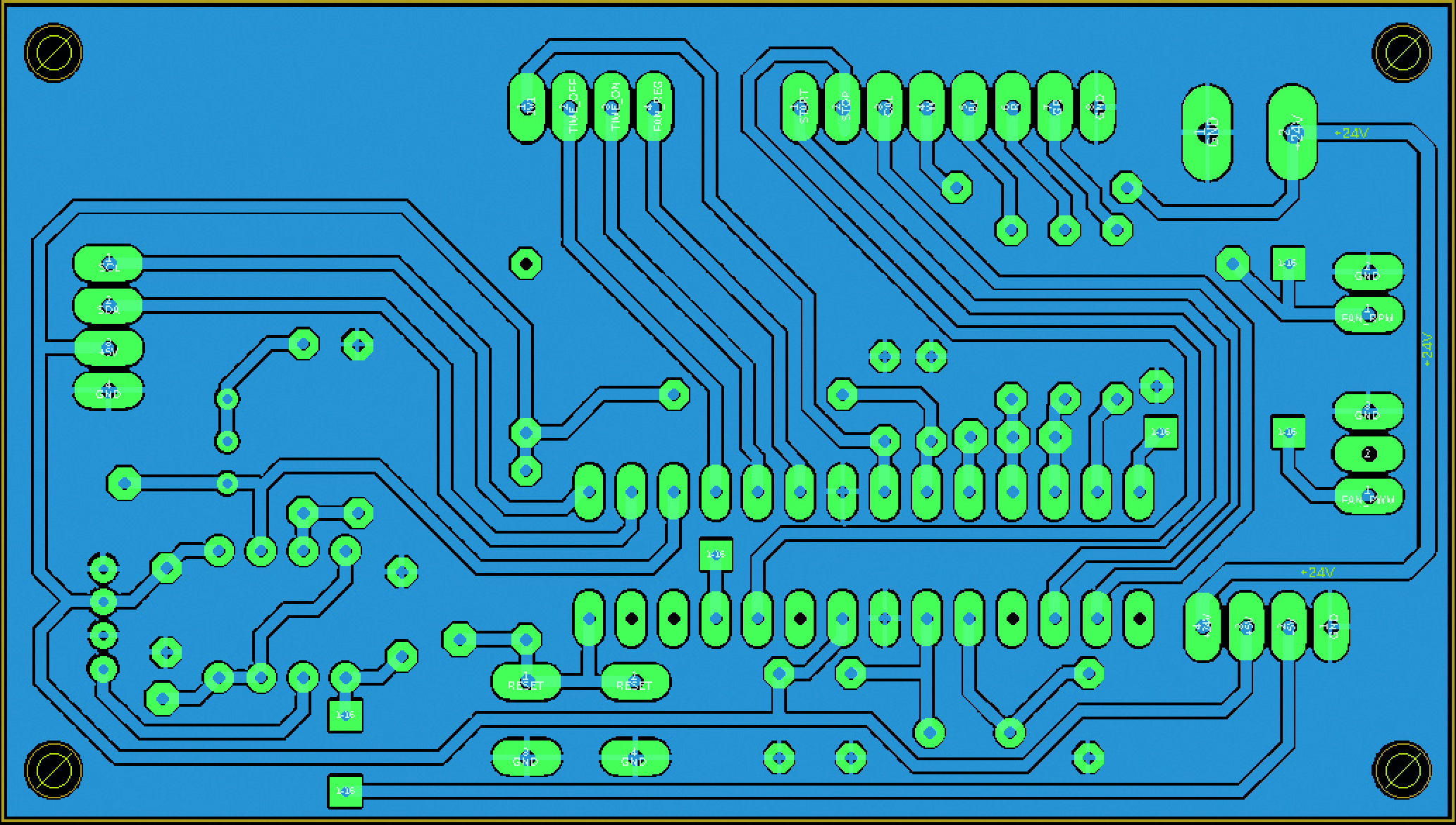
Preliminarily, you need to draw the circuit diagram and its PCB. Except in very rare cases, it is always convenient to equip the PCB with the so-called "ground plane," which not only connects all the ground points of the circuit, without the need to draw the corresponding tracks, but also fills all the empty spaces of the PCB; this will be very useful for etching. Otherwise, we would complicate our lives by having to remove all the excess copper, prolonging the etching time disproportionately, or by having to resort to setting up a series of isolated polygons, during the CAM processing phase. As an example, we will use the drawing shown in Figure 1.
The first operation to be done on the CAD program is to create a specific DRU file (this is what it is called in the case of Eagle) containing the design rules, basically the dimensions of the tracks and pads and their spacing, according to the type of PCB to be made. Indeed, one must consider that the typical default settings of CAD programs are fine for PCB fabrication at a professional service, but not for a handcrafted procedure. The parameters on which you have to act are, basically, the minimum dimensions of the connection tracks, pads (solder pads of the component rheophores) and vias (points of communication between the top and bottom faces of the PCB) and the distances between these components and between them and the ground plane, i.e., all the adjacent copper covering the remaining spaces of the PCB and which is grounded. If suitable values are not adopted, it may be difficult to solder components to the PCB. Let's look at these parameters and what values are appropriate to assign to them:
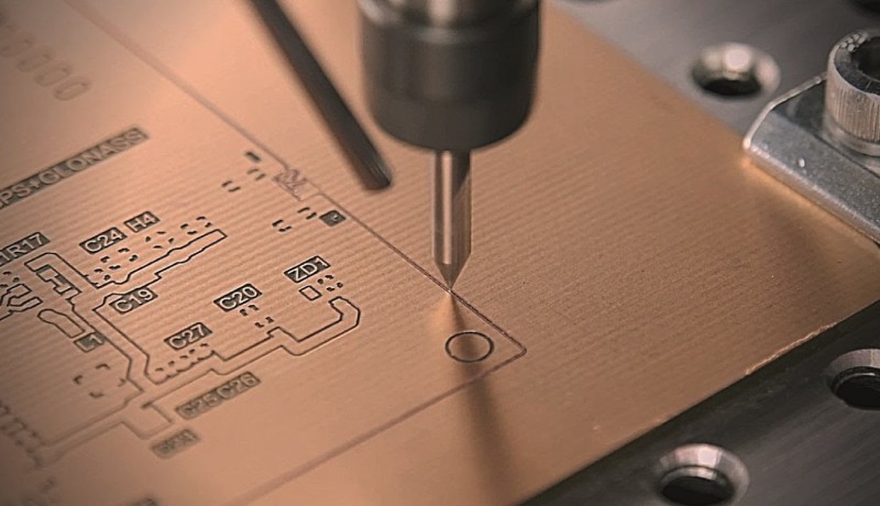
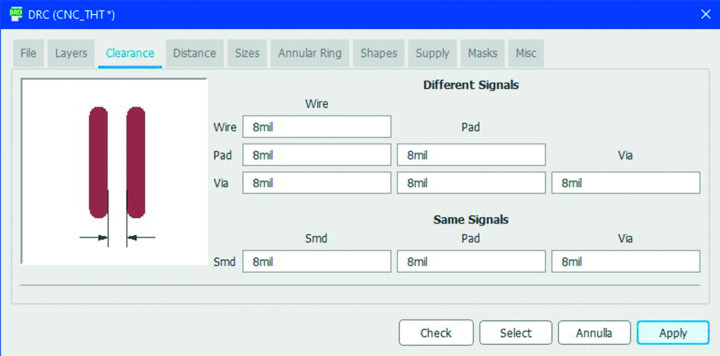
- Clearance: is the minimum spacing between the various components of the design: tracks, pads and vias. In our case, we used a value of 8 mils, equal to about 0.2 mm, which is a standard value also used for service; this means that you have to be fairly handy with the soldering iron; otherwise the tin can invade adjacent tracks or pads or the ground plane, causing short circuits. The value of 0.2 mm coincides with the size of the burin tip we used with our CNC, so one pass will be enough to remove excess copper from the copper plate, during etching (Figure 2). If you think you do not have sufficient soldering skill, then we recommend doubling this value to 16 mils; in this case you can use a 0.4 mm burin or always the 0.2 mm one, with which the CNC will make two adjacent passes. In any case, when soldering, a good help can come from the use of flux; passing it with a brush, before soldering, will facilitate soldering and prevent tin from touching nearby tracks or pads.
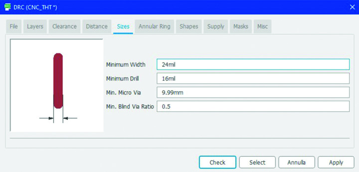
- Sizes: these are the minimum size of the tracks and the minimum diameter of the holes; by using too small a value for track width, you run the risk that a burr from the burin cut could generate extremely thin or even broken tracks. We used 24 mils, equal to about 0.6 mm, while the diameter of the holes is irrelevant for our needs, however a value of 16 mils is fine (Figure 3).
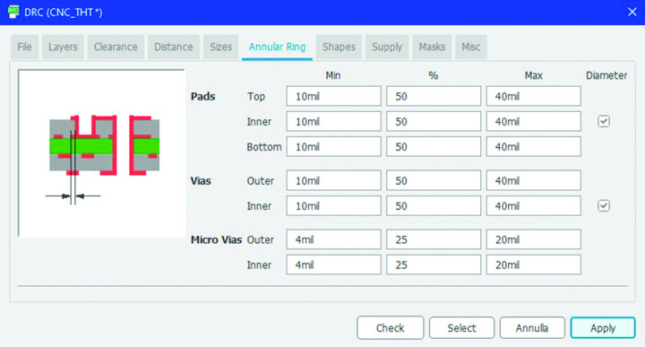
- Annular ring: these are the dimensions of pads and vias; the standard values from the libraries of the various components are fine for a service, but when operating with CNC, easily the outer edge loses something, while drilling without metallization removes more material in the central part; this can result in excessive reduction of the soldering space around the rheophores, with the difficulties that follow. The dimensions are defined as a percentage of the inner diameter of the hole, within a minimum and a maximum value. For pads, these values can be set separately for the top, bottom and inner surfaces of the copper plate, but the latter value is irrelevant, since it can be used only for professional multilayer PCBs, which are not realizable by craft techniques. As for vias, the dimensions are unique for the two outer faces, while the same applies to the inner value, as for pads. Microvias also fall within the professional types. In our case, we set a size increase of 50% over that provided by the component libraries, with a range of values between 10 and 40 mils (Figure 4).
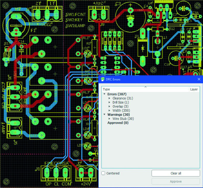
You will find the CNC_THT.dru file here: How To Mill Your PCB Tracks Instead Of Etching Them"], which should be copied to the dru folder in Eagle. Once you have opened the PCB drawing file, you need to use the Tools-DRC… menu command, click on the Load… button and load the file. By clicking first on Apply and then on Check, Eagle will apply the settings and then check that the drawing has characteristics corresponding to those provided in the DRU, if not, a mask will open with all the errors found. In Figure 5 we intentionally applied a DRU for CNC to a PCB design made for printing at a service. The result is that of as many as 387 errors and 30 warnings. Specifically, we have:
- 31 Clearance: means that in 31 cases, the minimum distances between tracks were not respected;
- 1 Drill Size: means that in one case the size of a hole is smaller than the minimum expected size;
- 5 Overlap: means that there are 5 problems with overlapping tracks, due to the fact that the DRU settings used increase the size of the PADs and overlap them with each other; actually this error would come out even with the correct DRUin fact, we caused them voluntarily;
- 350 Width: means that in 350 points the tracks do not meet the minimum size set by the DRU;
- 30 Wire Stub: these are repeated repasses in some places of the tracks, it happens easily when we erase a track to recreate it, but we do not realize that we have not erased it completely, especially within PADs.
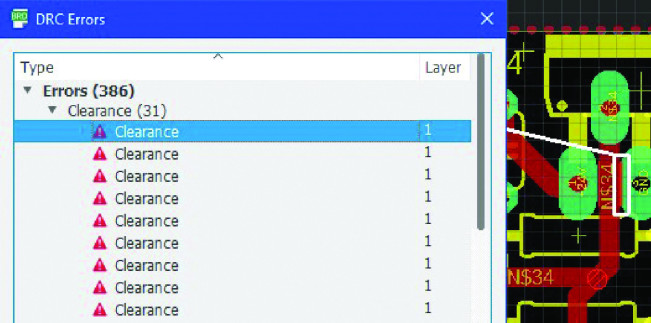
Eagle helps us find and remove errors, as we just select them individually and a highlight box will open, indicating the point or section affected by the selected error. Figure 6 shows precisely the indication of a clearance error-the track passing between the two PADs is too close and does not meet the parameters of the DRU; therefore, it must be reduced or moved until the error is eliminated. In some cases, you may decide that the error indicated by the DRU check is irrelevant to the making of your prototype, in which case you can select that error and click on the Approve button so that it is removed from the list, but this option should only be used if you know exactly what you are doing; otherwise you may then have problems in etching and probably in the operation of the circuit after the components are assembled.
Gerber File Generation
Once you have removed (or approved) any errors indicated by the DRU, you can move on to the stage of Gerber file creation, a fairly simple operation with Eagle.
The following is the list of steps:
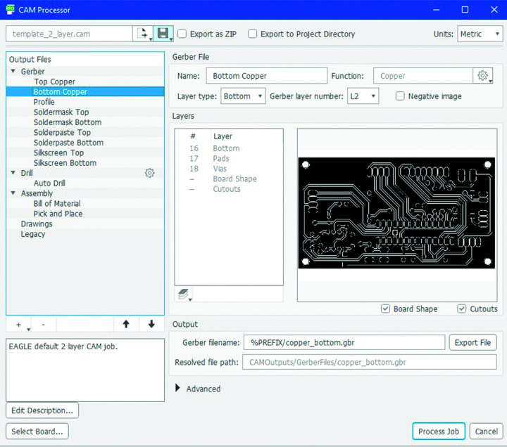
- Click on CAM Processor (Figure 7);
- Select TOP COPPER to check the preview of the top face of the PCB (useful for double-sided SMT or THT circuits);
- Select BOTTOM COPPER to check the preview of the top face of the PCB (useful for single-sided THT);
- Activate Board shape to get a border around the PCB (will be useful when final cutting the PCB);
- Activate Cutouts to get the inner circles of the large holes; DO NOT touch the Advanced section, which is basically for mirroring THT PCBs, we will treat it using FlatCAM;
- Click on Process Job: instantly Eagle creates, in the selected location, the folder CAMOutputs with all the files needed for processing the PCB by a service.
You can leave the folder where it was created or move it to a more convenient location, for the next steps.
Track CAM File Generation
After installing FlatCAM you need to run it and, just the first time you use it, you need to perform these simple steps:
- Go to the blank line located at the bottom of the program shell (Figure 8);
- If the shell is not visible, run the command Tool ⇒ Command line;
- type get_sys excellon_zeros and press ENTER on the keyboard;
- write set_sys excellon_zeros T and press ENTER on the keyboard;
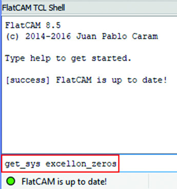
These two lines of code are needed so that you can see the holes clearly when you load a drill type file; we will discuss this later. This operation permanently changes the program options, so it should not be performed again in the future. At this point, you can also close the shell to leave as much space as possible for the main pane, just run the Tool ⇒ Command line command again.
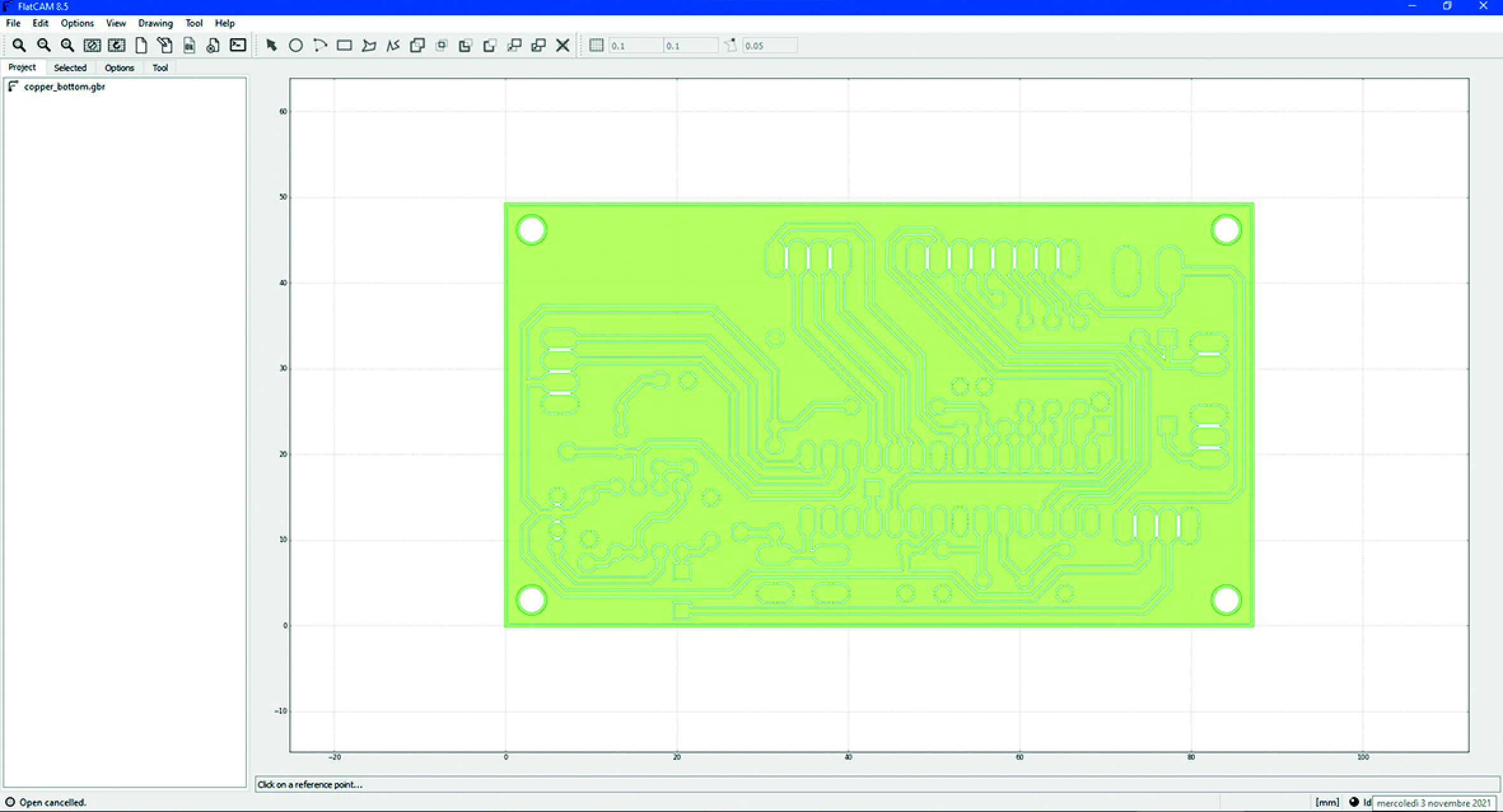
Run the command File ⇒ Open Gerber… and look for the file to open in the CAMOutputs/GerberFiles folder, since we are working with a single-sided THT circuit, we are only interested in the bottom one (file copper_bottom.gbr), in the case of SMT circuits we would need the file copper_top.gbr. Figure 9 shows the type of image you will see in the middle pane after the file is loaded.
Open the Options tab and set the Units field to mm. Since the PCB drawing is always made from the component side, as it is, the engraving would be reversed, so mirroring must be done. We need to run the Tool ⇒ Double-Sided PCB Tool command and set these parameters (Figure 10):
- Bottom layer = copper_bottom.gbr;
- Mirror axis = Y;
- Axis location = Box;
- Point/Box = copper_bottom.gbr;
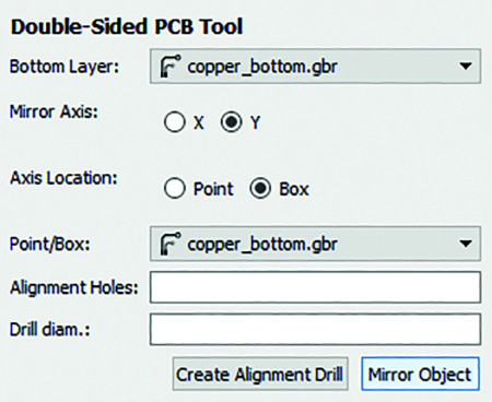
Click on Mirror Object, the PCB will now be visible directly from the solder side (bottom face).
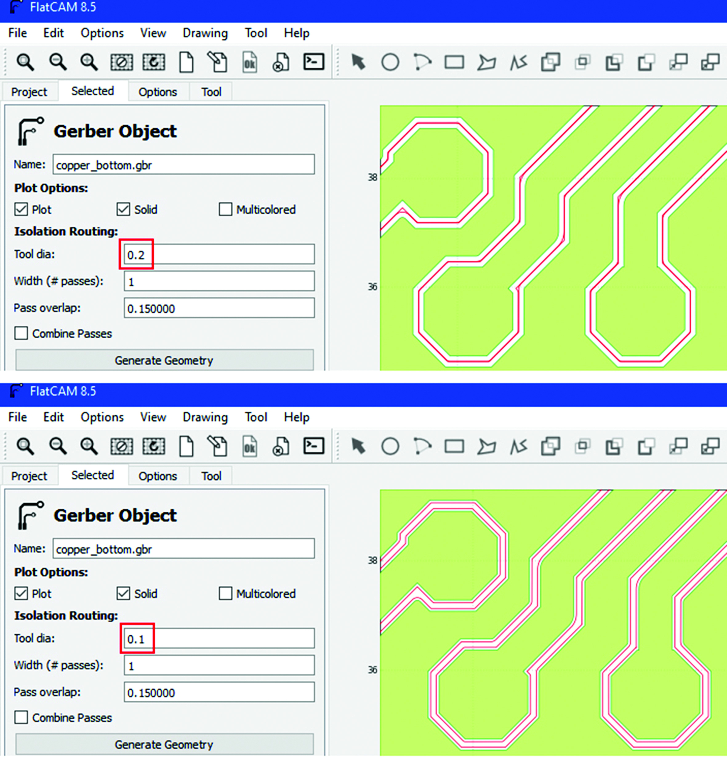
Please note: Of course, the Tool tab will not have to be changed in case we need to work with the top face (SMT circuits). Open the Project tab and double-click the copper_bottom.gbr project, the Selected tab will open, we need to set all the following options:
Plot options:
- Activate the Plot and Solid boxes.
Isolation routing:
- Tool dia: Here we need to enter the diameter of the burin tip that we will use for engraving. The DRU we have used provides for a distance between the tracks, or between the tracks and the ground plane, of 8 mils (about 0.2 mm) so we need to choose a burin with a diameter equal to or submultiple of that value; we have 0.1 mm and 0.2 mm burins. If we adopt the 0.2 mm burin, the CNC will make a single pass engraving exactly the space provided by the DRU; on the other hand, if we use the 0.1 mm burin, the CNC will automatically make two passes side by side to engrave the same thickness; we set 0.2.
- Width: is used to increase the track isolation; it makes sense to use this field when there is no upstream action on the DRU applied to the PCB, but in our case we set it to 1 (single pass). If a larger number of passes is set, the FlatCAM creates a grbl file for each pass, so it is necessary to etch the PCB multiple times; with each new pass, the burin is shifted by a fraction equal to the value given to the next Pass overlap field. For example, if the isolation provided by the DRU is 0.2 mm, but we want to increase it to 0.3 mm, having only the 0.2 mm burin, we set this field to 2 and the next field (Pass overlap) to 0.5 (50%), so that the second pass is 50% overlap with the first pass, consequently the second engraving will be 0.1 mm.
- Pass overlap: this field is used only if Width exceeds 1; otherwise, it is ignored.
- Combine passes: it may be useful to enable this option, when Width>1, in when FlatCAM generates a single file instead of a number of files equal to the Width value.
- By clicking on Generate Geometry, a red line will appear inside the isolation traces, indicating that one pass will be sufficient to remove the excess copper; in Figure 11 we have enlarged the image, and simulated both the use of the 0.2 mm burin (above) and the 0.1 mm burin (below) to make it obvious that in the second case the CNC will have to make two passes to ensure the isolation expected by the DRU.
In case you notice any error after performing the generation operation, you need to perform these steps:
- Open the Project tab;
- Select the project copper_bottom.gbr_iso just created by the program;
- Press Delete on the keyboard to delete it;
- Double-click on the copper_bottom.gbr project;
- Repeat the previous sequence of operations.
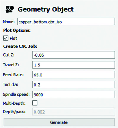
If everything is okay, however, open the Project tab and double-click on the copper_bottom.gbr_iso project; the Selected tab will open again, and you will need to set the following values:
- Plot: activate the box;
- Cut z: engraving depth in millimeters; usually the copper thickness is 0.035 mm, so you need to enter a larger value, also considering spindle movement tolerances, usually -0.06 to -0.08 is fine;
- Travel z: is the lift of the burin during travel, when not engraving, 1.5 mm can be set;
- Feed rate: engraving speed in mm/min, a low-value takes a long time but provides great reliability, a high value generates fast engraving but with some risk for the burin or loss of steps; we found a good compromise with a value between 50 and 80;
- Tool dia: 0.2 (same as the value entered above);
- Spindle speed: maximum rotational speed of the spindle; this value is for handling the PWM signal generated by the CNC controller; our model provides for this possibility, and from the datasheet of the spindle we get that at 36 V it can reach 9000 RPM, so we enter that value. If the controller you use instead has simple relay switching, this field can be ignored and remain blank. (Figure 12).
In case you notice any errors after performing the generation operation, you need to perform these steps:
- Open the Project tab;
- Select the project copper_bottom.gbr_iso_cnc that was just created by the program;
- Press Delete on the keyboard to delete it;
- Double-click on the copper_bottom.gbr_iso project;
- Repeat the previous sequence of operations.
If, on the other hand, everything is OK, open the Project tab and double-click on the copper_bottom.gbr_iso_cnc project, the Selected tab will open again, we need to activate the Plot option and enter the Tool dia field the same value used in the previous masks (in our case 0.2), then click on Update Plot, wait a few seconds, even if apparently nothing happens, then click on Export G-Code and save the file as Name_PCB.nc, where Name will be the name of your project; it is not mandatory to give a specific name, but if you do, you can create a folder containing all your files, for future use; the only thing essential is the ending .nc, otherwise, the file will not be seen by the Candle software.
Having reached this point, if your design involves SMD components, and therefore there are no holes, you can close FlatCAM and go directly to the engraving stage; otherwise you must continue with the next step of this program.
CAM Holes File Generation
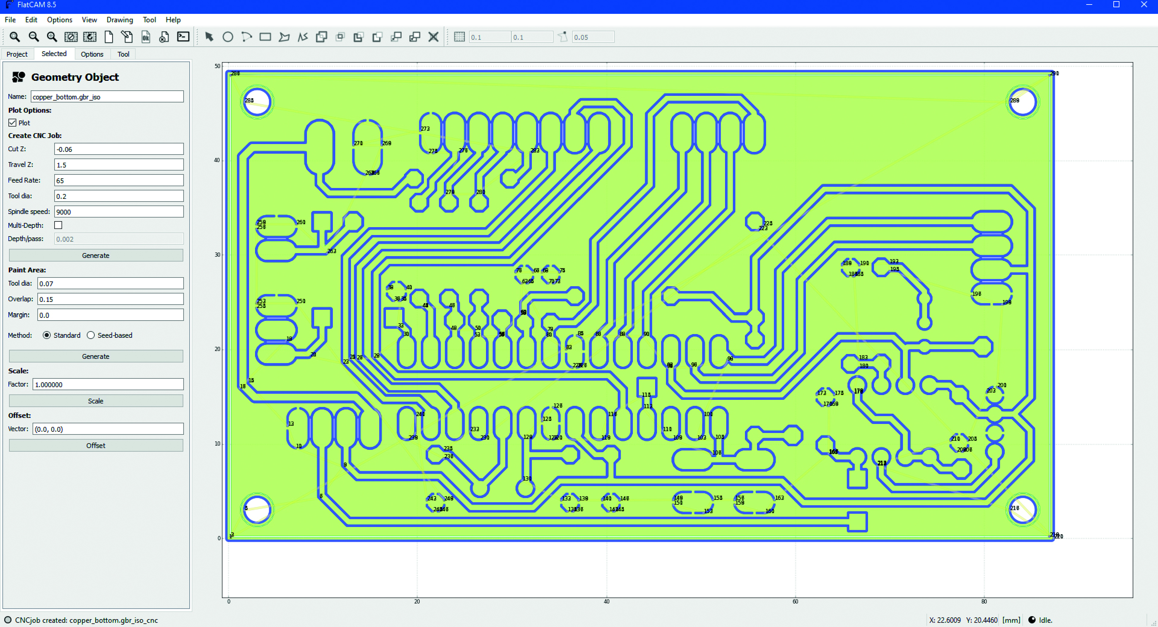
Run the File ⇒ Open Excellon… command and open the file drill_1_16.xln, found in the CAMOutputs/DrillFiles folder. If you have previously mirrored the PCB, you will see that the holes (represented by red circles) will not match the underlying pads or vias (Figure 14); You need to run the Tool ⇒ Double-Sided PCB Tool command and set these parameters:
- Bottom layer = drill_1_16.xln;
- Mirror axis = Y;
- Axis location = Box;
- Point/Box = copper_bottom.gbr.
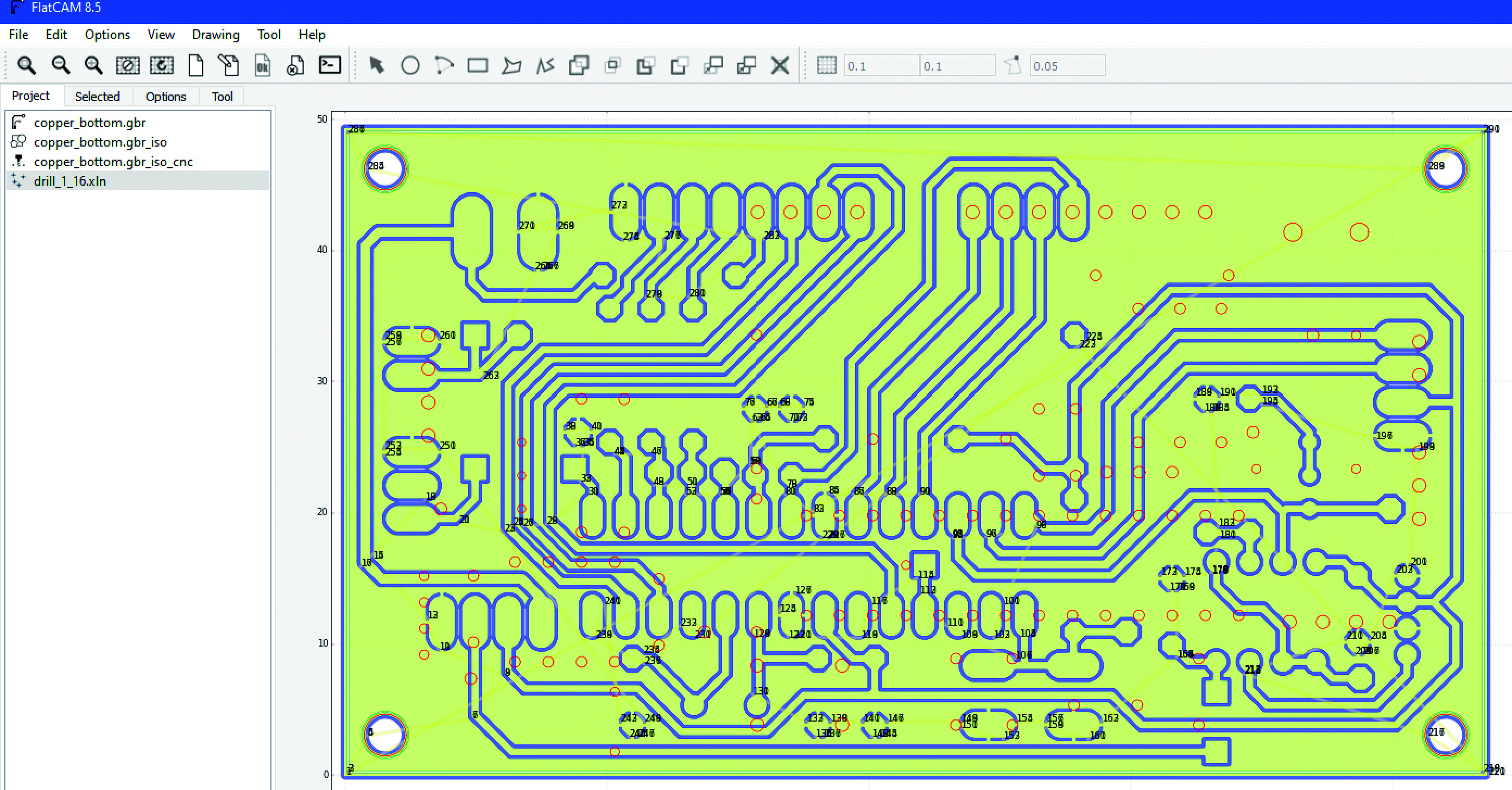
Click on Mirror Object, instantly the holes will be perfectly centered regarding the underlying pads and vias (Figure 15). In case you notice any errors after performing the mirror operation, you need to perform these steps:
- Open the Project tab;
- Delete the project drill_1_16.xln by pressing Delete on the keyboard;
- Run the command File ⇒ Open Excellon… and open the file drill_1_16.xln
- Repeat the previous sequence of operations.
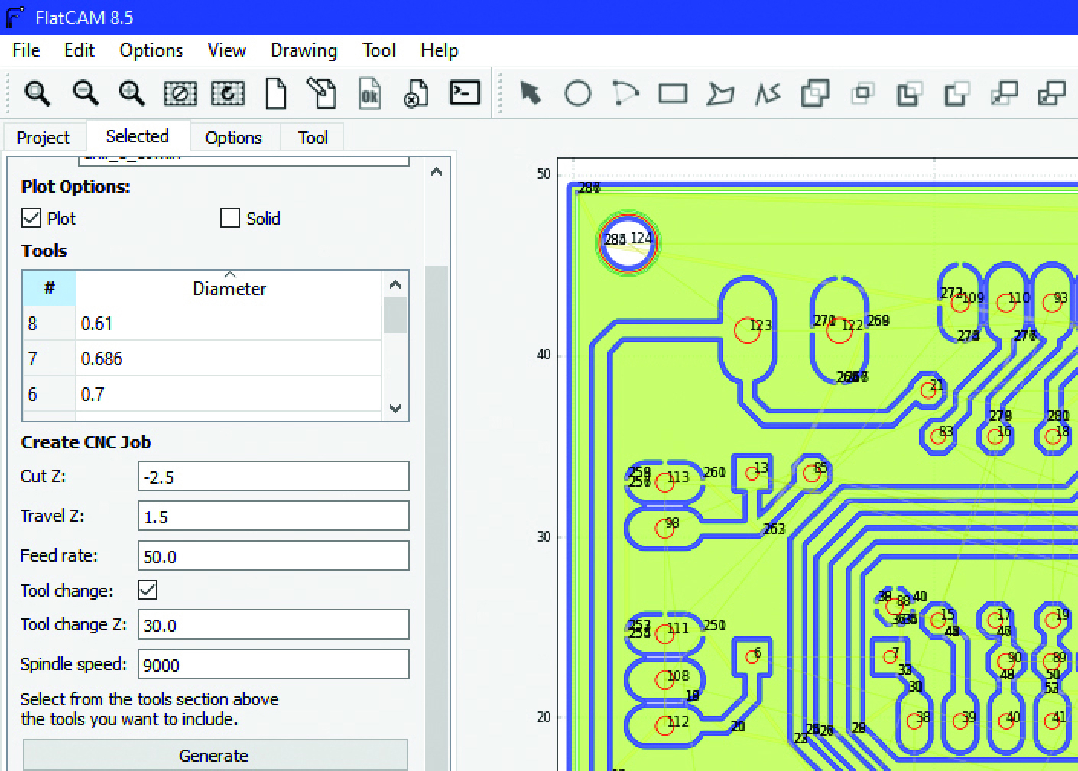
If everything is okay, however, open the Project tab and double-click on the drill_1_16.xln project, the Selected tab will open again, and you will need to set the following values:
Plot options
- Plot: activate the box;
Tools
- Tools: check the order of the diameters, it must be increasing, otherwise click on #. These values are the diameters of the drill bits that will be required for drilling the PCB; as you will notice, some values are out of standard, but they are tenths or hundredths of a millimeter, the only thing you have to do is to round them off virtually and then use the bit of nearest value, at the time it will be required.
For example: for 0.61 you will use a 0.6 mm bit, for 0.686 and 0.7 you will always use the 0.7 mm bit;
Create CNC Job
- Cut z: depth of the drill hole; PCB typically is 1.6 mm, the value to be entered is typically -2.5, if the PCB will be fixed on supports elevated above the plate, as in our case; Select all tool IDs with the mouse, which is critical for generating the grbl file;
- Travel z: mm of bit lift to move to the next hole, set 1.5;
- Feed rate: speed of the Z-axis during drilling, in units per minute; the program suggests a value of 3.0, but for our purposes you may well set a value from 30 to 50;
- Tool change: activate the box so that the CNC stops at each tool change;
- Tool change z: 30 (mm of spindle lift to allow bit change)
- Spindle speed: spindle rotation speed, the same as explained above applies, so for our CNC we set 9000, however, if you have another model of spindle, you need to refer to its datasheet.
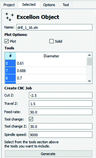
In Figure 16 we have shown the section just described with the values set.
Click on Generate, all holes will be numbered according to the drilling sequence (Figure 17); if this does not occur, totally or only for some holes, it means that the tool IDs have not been selected correctly. In case you notice any error after performing this last operation, you need to perform these steps:
- Open the Project tab;
- Select the project drill_1_16.xln_cnc just created by the program;
- Press Delete on the keyboard to delete it;
- Repeat the previous sequence of steps.
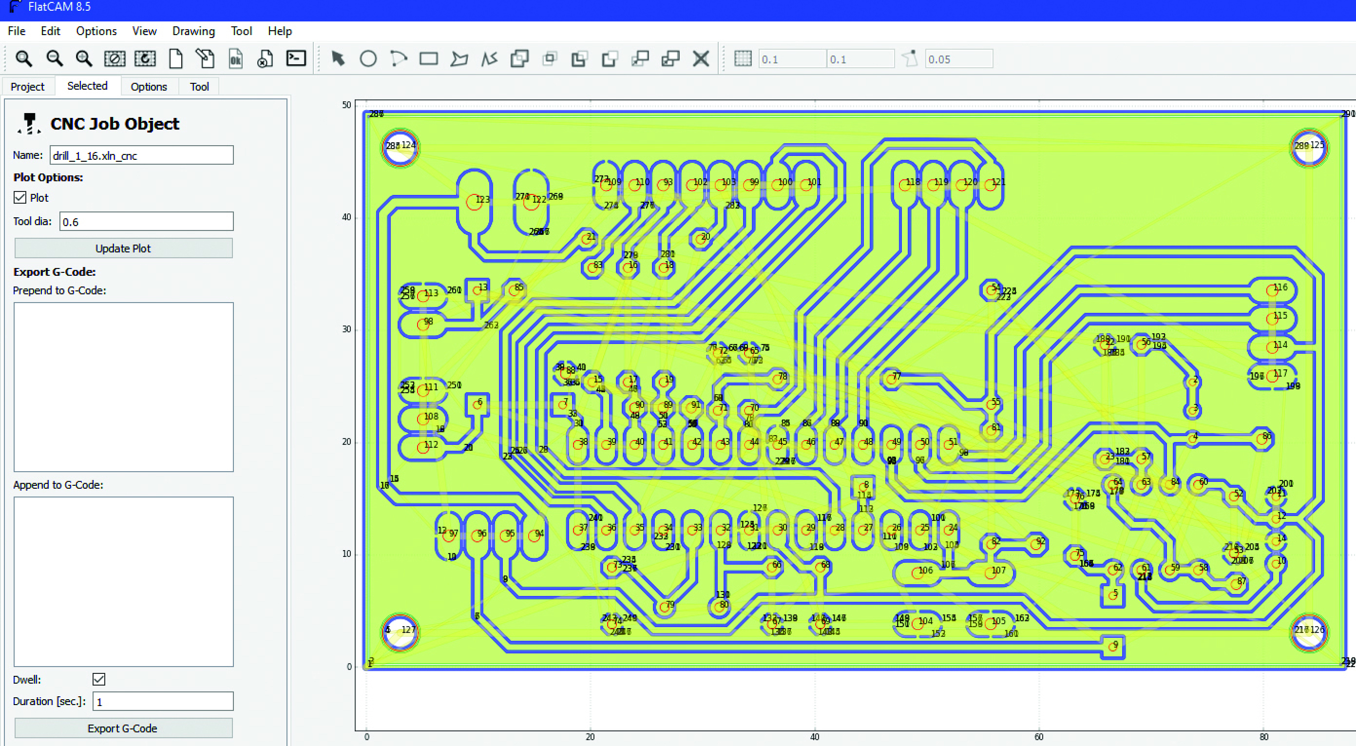
If everything is okay, however, open the Project tab and double-click on the drill_1_16.xln_cnc project, the Selected tab will open again, and you will need to set the following value:
- Tool dia: 0.6 (default initial drill diameter);
- Click on Update Plot; the image will now also show the drill path (Figure 18);
- Click on Export G-Code;
- Save with Name_FORI.nc, where Name will be the name of your project, as explained earlier for the track file; again it is essential to use the ending .nc, otherwise the file will not be seen by the Candle software.
With this last step, we have completed the CAM operations and now have two files in grbl format, with which we are going to machine our copper plate, first removing the excess copper and then drilling the necessary holes for the components.
Please note: It is important to save the FlatCAM project, perhaps in the same folder as the grbl files, so that you can reopen it to make quick changes to some parameter, without having to redo all the steps seen so far. The command to use is File ⇒ Save Project As…, providing path and name (usually the same one used for the two grbl files) such as Name_prj without a desinence, where Name will always be the name used previously. In the next installment, we will move on to the practical part, with in-depth study of the Candle program and making our first PCB.
Discussion (6 comments)