
PCB Tips and Tricks
on
Depending on your perspective, working style and previous experience, you might think that a custom PCB for a project should be ordered right at the start of the development process. You get an idea, draw a schematic, lay out the board, order it (or etch it yourself) and then assemble it. It’s often the case, even though the PCB is perfect, you have overlooked a problem at a completely different level. Now you need to order another followed by a third or even fourth. Each iteration takes a bite out of the project budget and encroaches on deadlines. To avoid this, I usually put off committing to the first PCB for as long as possible.
Build a Proto-PCB!
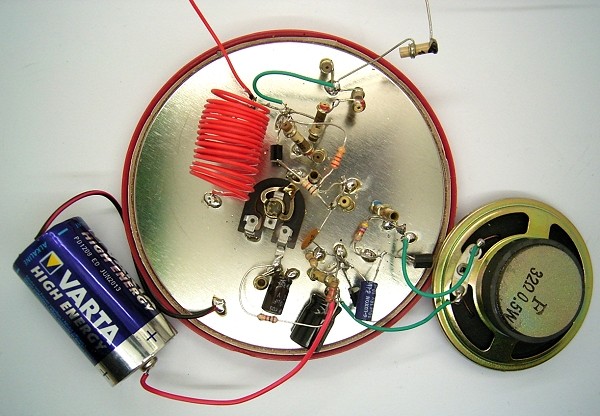
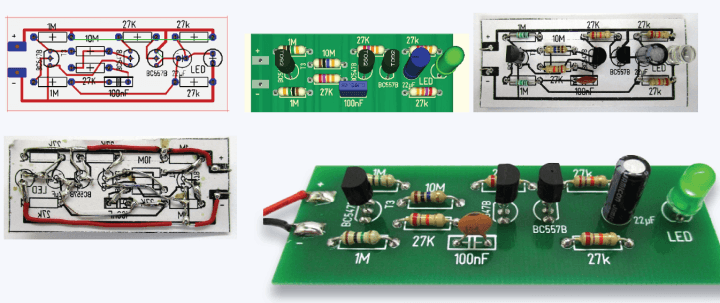
The circuit itself needs to be checked and tested somehow. No matter how much your first test setup looks like a rats nest, it will still provide vital insights into whether everything is working as it should. Components wired up on a standard prototyping plug board will often do the job here. Alternatively, you could use strip board, but I sometimes prefer the “hedgehog” structure built on a tin lid (Figure 1). This gives you a decent ground plane, and the soldered connections mean you don’t suffer intermittent faults from flaky connector contacts. Component values can be easily changed until everything works optimally. If the circuit proves to be unstable, you can work out the best place to site supply decoupling capacitors and small value capacitors to ground at points along the signal path.
When dealing with a microcontroller-based project, you would normally begin with an off-the-shelf development board. In this case, you can connect external components to provisionally test the overall function and develop the firmware. It is often easy to see whether you will need to include precautions for interference immunity. EMC problems reveal themselves by generating interference signals that you can hear on a radio. You may have already noticed that the circuit reacts badly to nearby sources of interference. This will indicate that special attention to interference immunity will be required in the board layout.
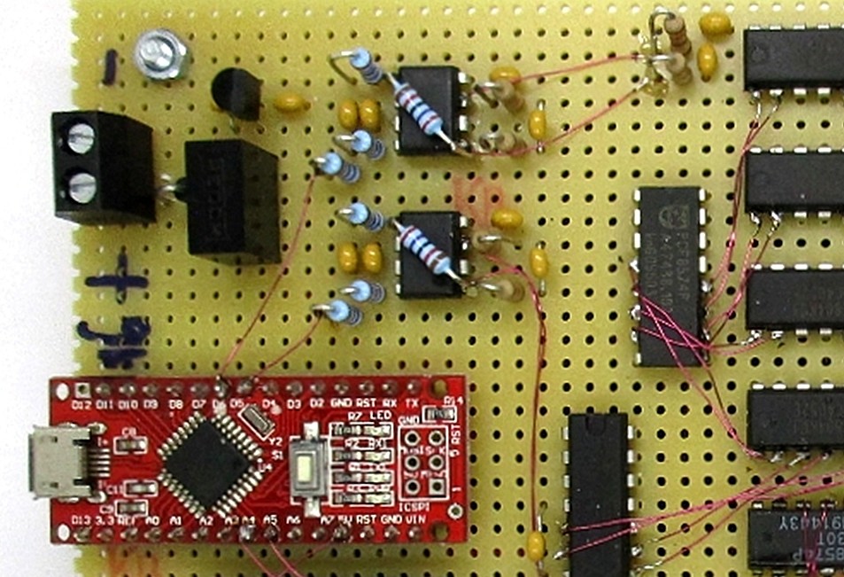
In many cases, I wire up the components on a breadboard to get a better idea of the finished board size and a possible placement of the components and any controls, as well as sockets for power and signals. This can then become a handy prototype (Figure 2). A client could even use it to carry out initial tests and suggest changes that can then be easily tested. Once the circuit has been finalized, you can then turn your attention to the PCB. Up till now wired components were probably used to build the circuit, but the final PCB will most likely use SMDs. The breadboard layout has probably not been EMC-optimized because there is no ground plane, but we now know what still needs to be improved.
Components and the Wiring Diagram
You probably already have circuit diagrams in the form of sketches. But all PCB design software tools require the input of the circuit diagram first. Each component needs to be specified very precisely. “Resistance 10 kΩ” won’t do, you have to detail the package, e.g. an SMD resistor of size 0805. Choosing the right components is often very time-consuming because there are so many similar components. This applies above all to connectors, switches, potentiometers and the like. It’s also necessary to determine that the chosen component is actually available and to be sure that its outline on the PCB layout is correct. It’s so frustrating to find your beautiful, pristine PCB has wrong hole-spacing and the USB socket will not fit on the board. Be very careful when selecting the components.
One thing I have found when working with SMD resistors and capacitors is they look so large and manageable on screen that it’s easy to misjudge their actual size. This can be a problem if you intend to populate the board by hand. The smallest components are problematic, at least when soldering by hand. You should have a few examples of the parts at your desk to perform a quick reality check. I, personally, find the 0805 outline easiest to solder. I remember a project designed using 0402-size components to save space. It proved extremely difficult to solder the components to build the prototype, but this situation can, of course, be avoided if the PCB is delivered assembled.
Once all the components have been selected, the circuit diagram can be drawn with all the connections. Incidentally, if an error occurs later when drawing the circuit board, you always have to go back to the circuit diagram and make the changes there first. The board layout software always ensures that PCB track layout matches the circuit diagram.
The PCB Layout
Now to the circuit board. First, you need to check the physical space into which it must fit to determine the dimensions and whether a double-sided circuit board will be necessary. You can now define features such as rounded corners and special outline shapes. You can change these later, but it’s easier if you get the measurements right from the start.
Double-sided boards are usually standard. A single-sided circuit board has hardly any cost advantages, but it can simplify the process if you intend to etch it yourself. In most cases, at the first stage, I will just order five or ten samples from a PCB service provider to save myself the hassle. Some PCB suppliers also offer to assemble prototypes. In this case, make sure in advance which components will be fitted and take this into account when creating the circuit diagram.
Once the outline is defined, you can import all components from the circuit diagram and initially place them on screen next to the PCB outline. You can then move them one by one onto the circuit board and look for the right placement, resulting in the shortest and most direct PCB track. Here it is an advantage if you have already built everything on a breadboard beforehand. You then already have an idea how to position the components with minimum number of crossing tracks so that vias to the other side can be avoided.
When all components are placed, you can start the auto router. The software then tries to connect all components as in the circuit diagram. However, it can then easily happen that the line routing is suboptimal from other points of view. There could be too long and tangled ground lines, or the “shortest” path between VCC and GND via a bypass capacitor becomes too long and forms an effective loop antenna. EMC problems are then inevitable.
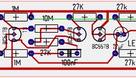
You should at least lay the ground and supply lines yourself in advance, and only then start the auto router. I go one step further and prefer to route all lines by hand. Above all, very simple circuits usually have a clear structure (Figure 3) and can be easily implemented.
Ground Planes
Continuous ground planes are a great help. For this, you can create a continuous copper surface on the underside of the circuit board connected to GND. All signal-carrying tracks stay on top as much as possible. Where it is unavoidable where two tracks cross, one track ends in a pad with a plated through hole (via) which routes the signal downwards to a small track on the lower plane and then upwards again at another point. It makes sense to establish a system with the track layout, perhaps running all the supply tracks horizontally and the signal-carrying tracks vertically as much as possible. Any break in the ground plane should be as short as possible to minimize voltage drops. Ultimately, a continuous copper plane helps to achieve the shortest possible route to ground over the entire board area; a through-hole connection is all you need when a component needs a connection to ground.
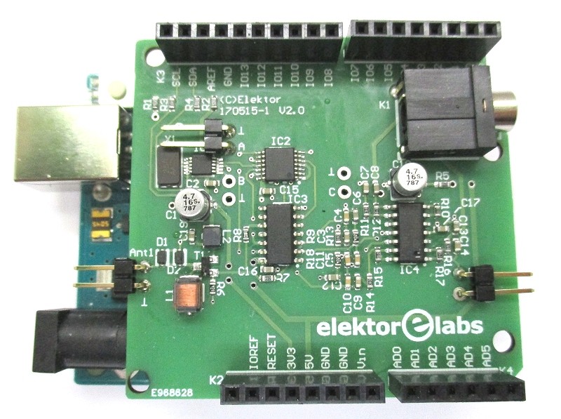
Ground planes can work wonders, as witnessed with the Elektor SDR-Shield (Figure 4) project. This circuit is a sensitive shortwave receiver, so it’s important to avoid any interference that would compromise its performance. The shield plugs directly over an Arduino Uno. At first, I was worried that mounting it so close to a microcontroller might give trouble, but it all worked out fine with trouble-free reception. A ground plane on the underside acts as a shield to signals from below, and interference fields from above have less of an effect because most field lines end directly at the ground and very few on the thin conductor tracks.
Connectors
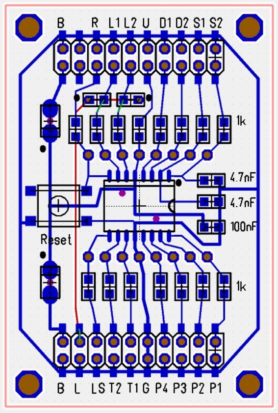
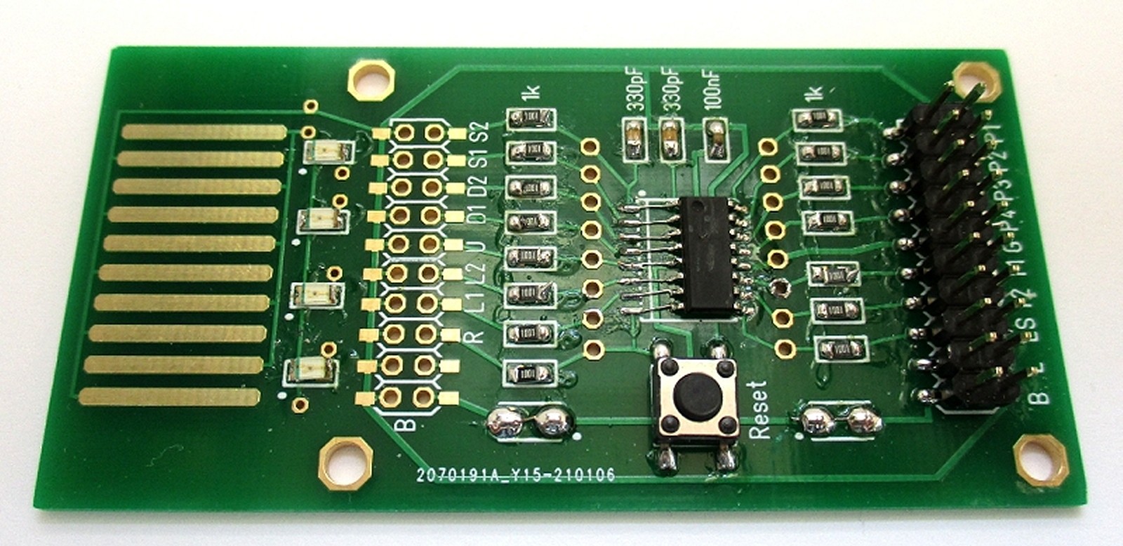
Most circuit boards need some connection to the outside world. Post plugs or sockets are often used on the edge of the circuit board, as with the Arduino, or other standardized plug-in systems. When it comes to experimental projects or circuit boards for education, larger connection points are often more practical. Round, through-plated 4 mm holes will accept banana plugs directly as well as crocodile clips (Figure 5).
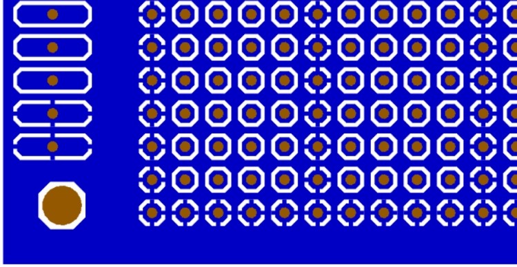
I like to specify double-sided, rectangular pads with through-plated holes spaced at 5.08 mm. These connection points do not add any additional costs and can be used very flexibly; you can solder wires, use crocodile cables or fit a screw terminal block. For very simple experiments, components can even just be plugged directly into the contact holes (Figure 6).
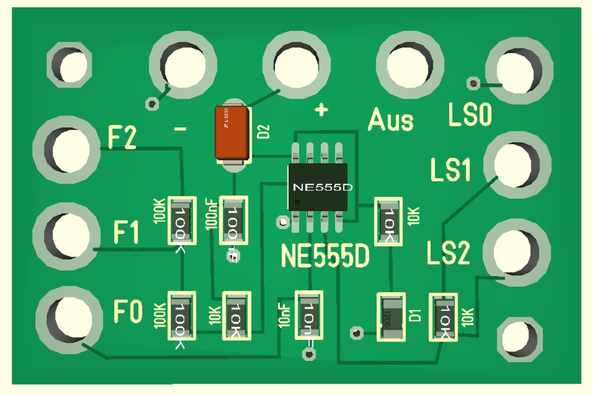
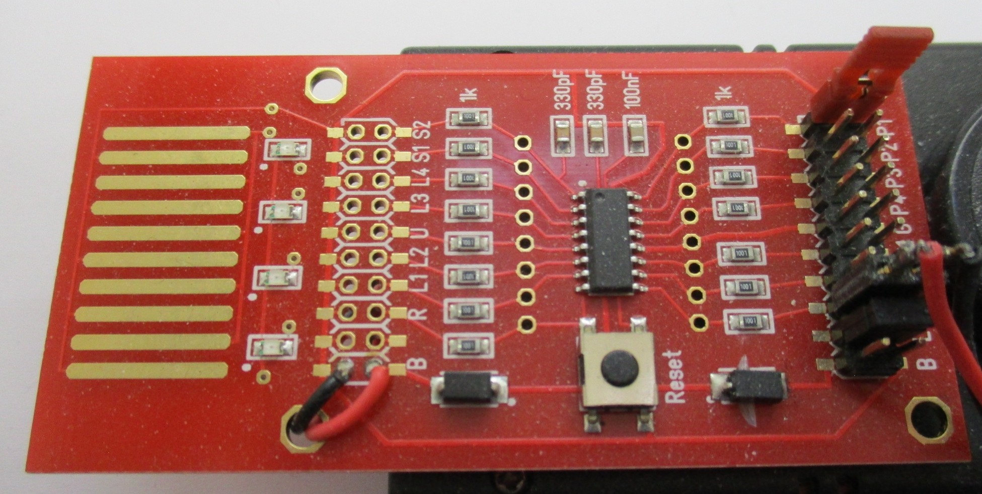
There are also PCBs that only consist of connection points. Then you don’t need a circuit diagram and can start right away with the circuit board. For an HF-capable breadboard, I created a continuous ground plane on both sides. Most of the contact points are on isolated islands. But the points at the edge of the field and several continuous rows are connected to earth (Figure 7). In this way, the earth is easily accessible everywhere by a short route, and you have a relatively good shielding surface.
Checking the Board Layout
Software used to make PCBs will run automated tests to find open circuits, short circuits and close parallel tracks. There are however other mistakes that can occur on a completely different level, which you will only be able to find out by yourself. The aim is that the first printed circuit board you order should be error-free, but as you know, Murphy’s Law applies here also. Looking back, I estimate that every second PCB I received has had a least one error. Last-minute changes are often the culprit here because they can generate a new unforeseen bug. There have also been errors made right at the project start which have somehow remained unnoticed.
To order a PCB, you have to convert the information into Gerber files. The software creates individual files for the different layers of the circuit board and for the drill holes. You can find various Gerber viewers on the web, which you can use to view the result. You can then switch between layers and get a completely different view. This is another important stage in the verification process and has uncovered many a missed bug, even at this stage there is still some uncertainty as to whether everything will work properly in the end.
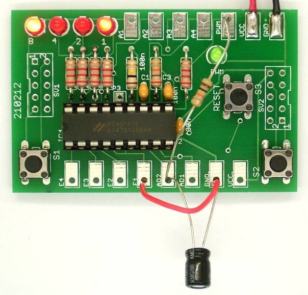
Another tip that can help to spot errors is to print out the layout and place the components over their outline. On one project I was working on, I thought I could skip that because the PCB was so beautifully simple and clearly structured. With the freshly unwrapped PCB on the bench and the soldering iron up to temperature, it suddenly hit me: Wrong SO outline package for the microcontroller housing! This particular component is available in a narrow or wide outline. In this case, I still went ahead and assembled the PCB by extending all the pins of the controller on one side using small lengths of wires (Figure 8).
That is so frustrating; I can however usually console myself by finding other tweaks that would benefit the layout (in this case better labelling) so that a new PCB iteration is not a complete loss (Figure 9).
When it comes to very simple boards with wired components, e.g. for training projects, you can go one step further and actually build a version of the board in advance: Stick a paper copy of the PCB layout onto a small sheet of cardboard and poke holes for the component leads. The components can then be plugged through the cardboard and soldered underneath. Short lengths of wire are then used in place of the PCB tracks. This gives you a good chance of spotting possible errors. In addition, it leaves you with a usable prototype to test before committing to the final PCB layout (Figure 10).
Many of these strategies for designing simple circuit boards work really well with small, manageable, experimental projects, but obviously not so well with larger designs. The head of a large company may well lack understanding and pour scorn on cardboard layouts, thinking they are amateurish, a waste of time and that any competent professional engineer should be able to get it right first time. Well, in principle that’s true, but believe me - oversights and mistakes inevitably occur, and multiple drafts are often required, each time adding to the costs and threatening project deadlines. I can only say the technique described here has worked well for me; the emphasis should be on preliminary trials and testing so that fewer versions of the board need to be ordered.
About the Author
Burkhard Kainka worked as a physics teacher for many years before becoming self-employed as a developer and author in the field of electronics and microcontrollers in 1996. He runs the www.elektronik-labor.de and www.b-kainka.de websites where you will find many interesting small and large projects along with information on the basics of electronics. Burkhard is an avid radio amateur with the call sign DK7JD.
Questions About PCB Tips?
If you have any technical questions or comments about this article or PCBs, please contact the author at b.kainka@t-online.de or the Elektor team at editor@elektor.com.
Discussion (6 comments)