
The Birth of the Microprocessor: The Intel 4004
on
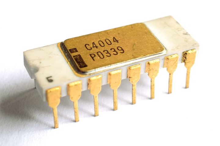
Having watched men land on the moon, seen the future described in animated series such as The Jetsons, and progressed from valve to transistor radios, there only seemed to be one invention outstanding – the microprocessor. Freshly founded and ready to ride the wave of the fledgling semiconductor industry, the task fell at Intel’s door. However, the accolade could easily have been grabbed by one of the many other industry players had it not been for the dedication and skill of Federico Faggin. Let's look at the history of the 4004 (Figure 1).
Before the 4004
In the 1960s, computing meant mainframes, such as the System/360 from IBM, with available processing performance shared across many users and programs. Memory was implemented using magnetic ferrite cores, and the available integrated circuits (IC) were primarily manufactured using transistor-transistor logic (TTL). Intel was convinced a future lay in metal-oxide-semiconductor (MOS) technology to supplant magnetic core memories.
In 1969, the Japanese Busicom corporation had asked Intel to develop a collection of ICs to form the basis of their first electronic calculator, the 141-PF printing calculator prototype [1 and 2]. Their approach used 12 chips, three of which formed the central processing unit (CPU). The goal was to develop a platform for electronic calculators that could be modified simply by changing the read-only memory (ROM) ICs. Intel’s team saw room to optimize the design, partly because the packages required didn’t match with their 16-pin standard in use at the time. A four-chip solution was proposed with the CPU integrated into a single package. The “Busicom Project” was thus born and, after some design work had been undertaken, the project sidled into inactivity towards the end of the year.
TTL was the technology of choice at the time, with a range of logic devices and memories available. MOS showed promise, capable of providing 10 times the density of TTL for the same cost and power dissipation. However, its speed was much slower, and it was generally considered to be unreliable. Intel had managed to bring a MOS static random access memory (SRAM), the 1101, to market, but early production could only yield two working die per wafer [3]. The speed issue was related to the capacitance of the gate caused by a combination of the use of aluminum and the manufacturing process. It had been determined that this capacitance could be reduced by using a silicon gate, enabling the gate to be “self-aligned” and the entire structure to be smaller. Unfortunately, the amorphous silicon approach used to date had proved brittle and prone to cracking during oxide steps.
MOS Matters
Federico Faggin moved to Intel in early 1970, having worked on MOS technology at Fairchild. There he had resolved a series of issues that were critical in making a microprocessor design possible. Firstly, using vapor deposition, he had replaced the amorphous silicon gate with polycrystalline silicon, leading to a much more reliable manufacturing process. Secondly, he’d developed a method for buried contacts that dispensed with the need for aluminum, resulting in denser circuity. And, finally, he’d created a bootstrap load approach that allowed for full and faster output signal swings than had been previously possible. The application of the technology to Fairchild’s 3708, an eight-channel analog multiplexer, had resulted in the design being four times faster, having 10 times lower leakage current, and two-and-a-half times smaller multiplexing transistors than the 3705, its predecessor that used metal gate MOS fabrication.
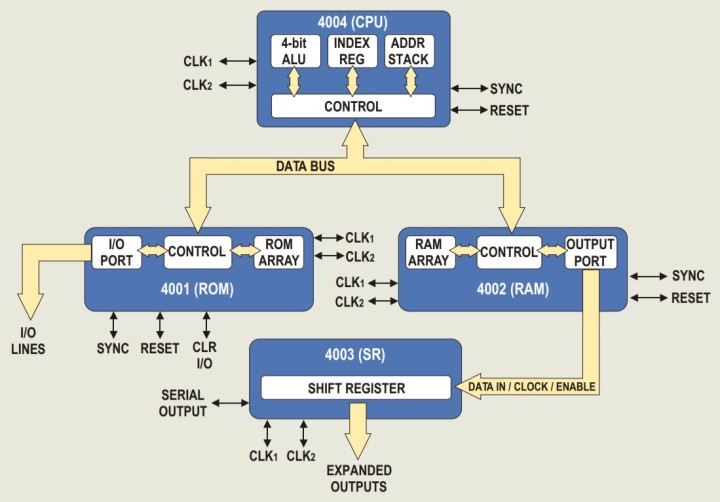
With Intel’s designers busy working on the 1103, their first MOS dynamic RAM (DRAM), Faggin was given what little there was of the Busicom project’s documentation and left to get on with it — on his own. The four chips consisted of the 4001, a 2048-bit metal-mask ROM; the 4002, a 320-bit RAM; the 4003, a 10-bit static shift register with serial in/out and gated parallel outputs; and the 4004 [4], a 4-bit processor whose design was incomplete. The 4000 product numbering used digressed from Intel’s standard approach. Still, it allowed the four chips to be perceived as compatible parts of a complete microcomputing platform that later became known as the MCS-4 (Micro-Computer Set) (Figure 2).[5]
Project Delays
The sudden arrival of Masatoshi Shima, Busicom’s lead engineer, just days after Faggin had started his new role, caused issues when Shima learned that the chips his calculator depended upon had not even been designed. Under pressure to meet Busicom’s timeline, Faggin agreed to supply a fully operational chipset by December 1970. The challenges were immense. Each device had to be designed and laid out by hand while also applying the latest MOS technology during the manufacturing process. Intel’s team was used to laying out memories whose features were repetitive, so the 4004 would push everyone to the extremes and test the limits of MOS fabrication.
Shima received permission to stay in the US for six months to support Faggin during the development. As the project proceeded, more and more designers and layout drafters were assigned. Around October, the first samples of the 4001 arrived, closely followed by the 4003. Both devices worked first time and even fulfilled the design targets set for clock speed and signal and supply margins. The 4002 required only a minor fix that was easily resolved.
First Tests
Shortly before New Year’s Eve, the 4004 was delivered. With the testing probe carefully lowered into place, the first die failed to work. Other die and then a further wafer also showed no signs of life. Careful inspection of the wafer using a microscope showed that the buried contact layer was completely missing, leaving most of the transistors’ gates unconnected. The delivery of a new batch of wafers, three weeks later, showed the design to be fully functional.
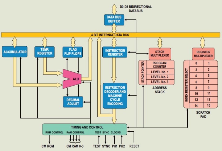
The 4004 was the first commercially produced microprocessor, operating at up to 740 kHz, with single-word instructions requiring 10.8 µs and two-word instructions needing 21.6 µs (Figure 3). With only 16 pins available, two were dedicated to a two-phase clock, two were for power, and two more were taken for reset and test. Four were assigned to a 4-bit, bidirectional data bus, one for a ROM select signal, and another to a sync output. The remaining four pins were used to select banks of RAM. The processor had no support for interrupts but did have a three-level stack. The 4001 ROM chips included a 4-bit input/output port, while the 4002 RAM devices had a 4-bit output port. The 4003 shift register was designed to interface with these ports. Together, these interfaces provided a method to interface with keyboards, printers, and other devices.
The 4004 Reaches a Wider Audience
The MCS-4 design was exclusive to Busicom, meaning that it could not be sold to anyone else. This proved frustrating to Faggin, who saw the incredible potential this freely programmable processing platform offered. To prove its potential beyond electronic calculators to Intel’s management, Faggin built a wafer-sort tester for the 4004 using the MCS-4 chipset. Busicom was also in financial difficulty so, when Intel offered them the chips for a lower price in exchange for annulling the exclusivity agreement, they accepted. And, with that, the MCS-4 and the 4004 became available to all.
Busicom used the MCS-4 chipset to build other applications, such as teller machines, cash registers, and billing machines. Other companies used it to power the first microprocessor-controlled pinball game “Flicker,”[6] a bowling simulator, electric typewriters, and even an early voting system. Faggin continued with processor design, picking up Intel’s 8-bit 1201 project, which became the 8008 processor and launched in 1972. Both processors received upgrades, delivering engineers both the 4040 and the 8080 in 1974. By this time, Faggin felt that Intel was only interested in microprocessors in order to sell their core product, memory. To focus on microprocessors, he left to form Zilog at the end of 1974, where he went on to develop the highly successful Z80 that helped usher in the home computing revolution of the 1980s.
Author's note: *A processor Intel C4004 without grey traces, licensed under Creative Commons Attribution-Share Alike 4.0 International: https://bit.ly/3xHF58S
Stuart Cording is an engineer and journalist with more than 25 years of experience in the electronics industry. You can read many of his Elektor articles at https://www.elektormagazine.com/cording.
This article first appeared in the special November 2021 edition of Elektor.
Discussion (14 comments)