[Partner Content] Paste stencil design is not black magic. Using the right tools and with some experience, PCB designers can learn the ropes and design stencils for their PCBs, shortening the time to manufacturing cycle.
Paste stencil design is not black magic. Using the right tools and with some experience, PCB designers can learn the ropes and design stencils for their PCBs, shortening the time to manufacturing cycle.
A critical preliminary step of any PCB surface mount assembly is accurate application of solder paste for proper component attachment. The most common method of applying solder paste is through the use of a solder stencil – a .004” to .008” (.10 - .20 mm) thick stainless-steel sheet with laser cut apertures (or openings). The stencil is laid over the top or bottom of a PCB and solder paste is squeegeed over the template depositing precise amounts of solder paste where needed.
Paste stencil design is typically done as a CAM processing step by the PCB assembler. However, anyone designing a PCB can design a paste stencil provided they have the tools and experience. Providing a stencil design to the assembler will reduce processing time and get PCB assembly started sooner. With proper tools and experience, stencil design can be performed well before a design is passed over to the assembler. Here are two common issues related to stencil design that can be easily assessed with CAM350® analysis and stencil design tools.
Paste remains on inner walls of stencil
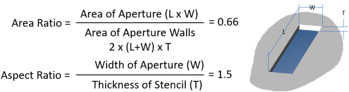
Proper release of paste from walls of a stencil as it is removed from the PCB surface requires compatible area and aspect ratios for the apertures. Area ratio is calculated by dividing the area of an aperture by the area of its aperture walls. Aspect ratio is calculated by dividing the width of an aperture by thickness of the stencil. Per IPC-7525 specification, an area ratio of 0.66 and aspect ratio of 1.5 is recommended. How to calculate area and aspect ratio for paste mask stencils
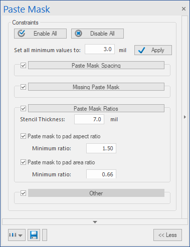
Our CAM350® and DFMStream® product can analyze two factors for all stencil apertures and identifying apertures not in compliance.
Ratio constraints in CAM350/DFMStream Paste Mask Analysis
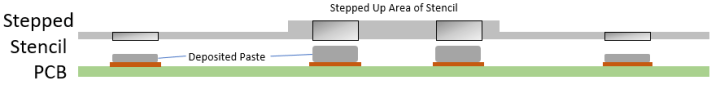
When PCB designs contain a mix of BGAs, QFPs, 1206 and 0402, a uniform aspect ratio is seldom adequate. For example, a BGA may require a greater volume of paste on its pads than an 0402. To resolve such variable aspect needs, stepped stencils are commonly used. Stepped stencils are stencils of varying thickness to accommodate varying volumes of paste. Stepped stencils increase volume and height of solder paste in selected areas and reduce it in others. Example of a Stepped Stencil
Solder beads (or balls) are present after final assembly
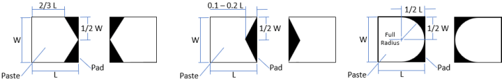
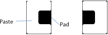
Having incorrect size or shape of paste on a component’s pad may lead to solder squeeze out resulting in random solder beads. For that reason, having a paste shape identical to a pad shape is not often desirable. At a minimum, the paste area should be proportionally smaller or different shaped than its pad. For many discrete packages such as 1206, 0805, MELF and others with rectangular pads, it is best to employ Homeplate, Bow Tie or Cpad paste shapes. Per IPC-7525 specification, here are recommendations for applying these shapes to chip style components: Homeplate Bow Tie (inverted Homeplate) Bullet
IPC-7525 Specifications for Chip Components
As you can see, the recommended paste shapes have less area than the pad shape. A cylindrical MELF package requires a different shape that provides a “pocket” where the ends can rest and prevent it from moving off center of the pad as the solder heats and cools.
Example MELF Cpad paste shape
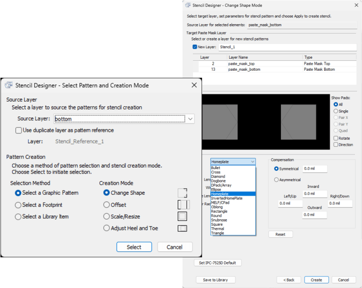
Creating these paste shapes or apertures can be tedious if your PCB Design tool does not offer paste stencil design functionality. CAM350’s Stencil Designer automates and simplifies the task of stencil design. Import a Gerber, ODB++, IPC-2581 file and select any paste mask, soldermask, top or bottom PCB layer as the source for component or pattern selection. Select patterns and choose to assign a pad shape from a collection of standard stencil shapes, or use offset and scale to create re-sized or repositioned shapes. CAM350 Stencil Designer
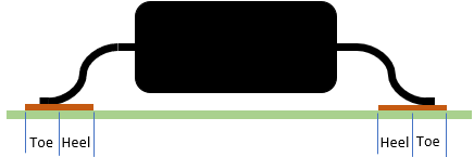
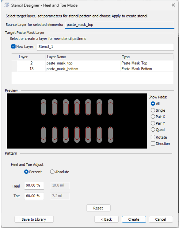
Use Heel and Toe creation mode for gullwing (i.e. SOIC) and J-lead (i.e. PLCC) patterns to distribute paste proportionally between heel and toe sections of the leads. In the example below, the paste shape is 90% of the inward half (Heel) of the pad and 60% of the outward half (Toe) of the pad. Our research has not uncovered a one size fits all for applying heel and toe percentages. The ratio varies based on the lead style of the component.
Create Heel and Toe based stencil shapes
Before starting a paste stencil design, you should discuss with the assembler to understand their requirements. They may standard component package-to-paste shape mapping to reference when creating the stencil design. Paste Stencil design a very repeatable process. Once you establish a component package-to-paste shape mapping, the mapping can be applied to all future designs having the same component packages. For that reason, CAM350’s Stencil Designer also offers stencil library support and fully automated stencil creation.
This is another example of improving the ‘handshake’ between design and manufacturing. Just as was done for Signal Integrity Analysis (SIA) and Design for Manufacturing (DFM) analysis, the design of the paste stencil can be brought upstream in the new product introduction (NPI) process, further streamlining preparation and handoff for manufacturing and thereby reducing overall time to market.
For more information about how CAM350® can help designing a paste stencil, please visit our website at https://www.downstreamtech.com/.

Discussion (0 comments)