
Adjustable Switch-Mode Power Supply (SMPS), 30V/3A max [150161]
Adjustable Switch-Mode Power Supply capable of delivering 30V and a maximum current of 3 A (5 A is possible, but with reservations).
In 2010 we published a power supply called UniLab (project 090786). It was able to deliver 30 V and 3 A. This design can be considered its successor. Maximum voltage is also 30V and the maximum output current is limited to a little over 3 A (5 A is possible, but with reservations). We used a different step down voltage regulator, the LM2677-ADJ. It has a higher switching frequency (260 kHz), which reduces the size of the output filter. The standard application only needs a few extra parts. But then the minimum voltage is basically the internal reference voltage (1.21 V) and we like the output to go to 0 V, well as close as possible to 0 V without the use of an extra negative supply voltage. As a source for the input voltage we chose a Mean Well DC power supply (but any similar DC supply can be used). It’s cheaper than a mains transformer, rectifier and smoothing capacitor. And you don’t have to worry about mains related problems, only a mains switch is needed.
The schematic may look rather complex, but not really. P3 sets the output voltage in combination with IC2B. IC2B is needed in the feedback of regulator IC1 to make the output voltage variable from (almost) 0 V to 30 V. IC2A amplifies the voltage across shunt R13..R16 so it can be compared to the voltage from P4. P4 sets the maximum output current. IC2D compares the actual output current with the setting of P4 and limits the output voltage by reducing the voltage from P3. R’s (3) and C’s (7) are added for compensation to suppress instability. Of course IC2 needs a power supply that’s independent of the output voltage. The LM6134 is a fast (10 MHz) rail-to-rail in-out opamp with a supply voltage range of 1.8 to 24 V. 5 V is more than enough here and since the power supply for the opamp is also the reference voltage for potentiometers P3 and P4. A LM317 (IC3) is chosen for a more stable 5 V. R34 and C17 filter out any artifacts coming from the input voltage. Also the maximum input-output voltage differential of the LM317 is 40 V, so it can handle the 36 V input voltage (or a little more) without any worries. LED2 indicates the presence of an input voltage. To make sure no ‘strange effects’ occur at the output when the power supply is switched off, T1 shuts down the regulator when the input voltage is too low. After 30 years or so I finally found an excuse to use a P-channel JFET. Advantage of the circuit comprised of D1/R1/T1? It doesn’t need an extra power supply to function except for the voltage it’s supposed to monitor. If the gate-source voltage of T1 is 0 V or very low the JFET will conduct and IC1 will be turned off, as long as the voltage at the input of IC1 is less than 0.8 V. Pin 7 has an internal pull-up current source of 20 µA. If the input voltage is high enough Zener diode D1 will conduct and the gate-source voltage will be positive enough for the JFET to get into a high impedance state. In our prototype the voltage across R1 at 36 V input voltage is 6 V. The voltage on the source of T1 is about 3 V. The J175 was chosen for its fairly low Gate-Source Cut-Off Voltage tolerance: 3 V min. and 6 V max.
Most important part of this design is probably the change of the feedback to IC1. To get the output voltage to 0 V, the feedback of IC1 has to be a little more positive than its internal reference voltage. With standard application this isn’t possible and the lowest output voltage is simply the internal reference voltage of 1.21 V. The concept chosen here is one of a DC amplifier. A control voltage from 0 to 5 V is proportional to an output voltage of 0 to 30 V. This way no extra reference voltage is needed. The feedback from the output has to be non-inverted so the control voltage is connected to the inverting input of IC2. The inverting gain is -1 and this means for the voltage from divider P1/R1/R9 an amplification of +2. If 30 V is set at the output the divider has to produce 2.5 V on pin 5 of IC2. So P1+R10 is roughly 11xR9. As said before the feedback has to have a positive offset to get the output to 0 V. Voltage divider P2/R8/R7 give R9 a bias of 0.66 V. This voltage is needed when P3 is set to 0 V to have 0 V at the output. Values of R7/R8/P2 are relatively low compared to R9. This way a change of the current through R9 has little effect on the voltage across R7 (we measured 0.657 V…0.678 in our prototype), but P2 should be adjusted for 0 V output voltage. The voltage across R7 at higher output voltages is of no consequence. Set P3 to minimum level and adjust P2 until the voltage increases. This can be done with or without a load. Without an external load the minimum output voltage is about 0.3 V. With a 12 Ω load for instance (can also be 8, 10 or 15 Ω) it’s only 11 mV. If P2 is adjusted without a load, adjust it so the output voltage is just about to increase. With or without the 12 Ω load, the voltage will stay at about 0.3 V. But if it is adjusted with the 12 Ω load it is possible to set the output to a lower value. In our prototype this lowest level was 11 mV. No load voltage won’t change and stay at 0.3 V.
To keep it cheap (main design specification) we didn’t use an accurate shunt to measure the current but paralleled four 0.1 Ω resistors (R13…R16). They have a 5 % tolerance and in our prototype the output voltage on K3 was about 3.4 % to low. But with an extra external voltage divider a meter can be adjusted to give an accurate reading. This tolerance however has no influence on the operation of the current control. IC2A amplifies the voltage across the shunt 20 times (with additional tolerance). There’s enough headroom now to cope with high current pulses (with low frequency) of far more than 3 A. At 3 A output current the voltage at the output of IC2A is 1.5 V. IC2D compares the voltage from P4 with the output of IC2A. Since we want a maximum allowable current of 3 A divider R24/R25 reduce the 5 V maximum voltage of P4 to 1.5 V. IC2 holds the balanced between an amplifier with a large gain (limited by R26) and a comparator. Too high a gain would produce an unstable current control. A MOSFET at the output of IC2 limits the voltage from P3. R6 is needed to prevent T2 short circuiting the 5 V power supply in case P3 is set to maximum. R5+R6 is equal to R4 to give IC2B an inverting gain of 1. A MOSFET is used for its low Drain-Source resistance . This resistance is less than 2 Ω with a Gate-Source voltage of 4 V. Divider R28/R29 make sure the voltage on the gate is high enough for LED1 to indicate the current control is (becoming) active.
Some loose change. R12 is a zero load resistor to prevent the output voltage from getting to high when there’s no or just a small load. It also keeps the regulation more stable then. Downside is the extra power loss (2.7 W at 30 V) and therefore reduction of efficiency. Resistors R11, R22 and R27 and capacitors C5, C9, C10, C11, C12, C13 and C18 are added to improve voltage and current regulation stability. There’s no real calculation behind the values and so maybe there’s room for improvement. Values were determined by using a variable switched load at different frequencies and different output voltage and current settings. R3 is primarily put between the output of IC2B and the feedback of IC1 because it’s probably not wise to connect the output of an opamp directly to the feedback of the regulator. This also gave the possibility to add C5. R2 and R6 limit switching artifacts.
Why limit the current to 3 A when using a 5 A regulator? When testing a first proof of concept a phenomena was detected that made us reduce the maximum allowable output current. When pulsing the output with the resonance frequency of the output filter we measured a current flowing in the inductor of more than 1.5 times the current of the pulse. At 3 A peak this would mean a current close to 5 A peak in the inductor. To prevent tripping the internal current limiting of the LM2677 we simply set the maximum output current to 3 A. The current limit is set by R25 and R24. In case you really want and you really need 5 A, change both resistors to 10 kΩ. The rest of the circuit can handle the current except for the fuse. Change it to 5 A. Keep current pulses to a minimum. Otherwise there’s a chance the output voltage will collapse permanently or irregularly.
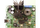
Mounting the parts shouldn’t prove to be difficult. Don’t forget to insulate D2 with a thermal pad and a bush, like the ones mentioned in the BOM. Also use a (very little) heat transfer paste between surfaces of IC1 and the heat sink, the thermal pad and D2. Put the head of the screw at the inductor side. We used a 10 mm M3 screw with nut and lock washer. IC3 doesn’t need to be cooled. Mount R12 at some distance from the PCB. The two potentiometers for voltage and current control P3 and P4 are not mounted on the PCB but connected with short thin flexible wire. Don’t make the wires longer than necessary. Be careful with the tab of the LM317 (IC3). It's connected to its output, so the 5 V power supply!
Features
- Switching frequency 260 kHz
- Max. Voltage 30 V
- Max. Current 3 A (3.2 A voltage limiting)
- Max ripple (260 kHz) 120 mVpp
- Low input voltage switch off 34.2 V
- Voltage drop (no load to 3 A) 0.17 V
- Efficiency (output 30 V/3 A) 93 %
- Efficiency (output 5 V/3.1 A) 80 %
Bill of Materials
Resistor
R1,R11,R28 = 10 kΩ, carbon film, 5%, 0.25W, 250V
R2,R34 = 100 Ω, carbon film, 5%, 0.25W, 250V
R3,R21,R30 = 1 kΩ, carbon film, 5%, 0.25W, 250V
R4,R9 = 20 kΩ, metal film, 1%, 0.25W, 200V
R5,R24 = 18 kΩ, carbon film, 5%, 0.25W, 250V
R6,R19 = 2k0, metal film, 1%, 0.25W, 200V
R7,R17,R18 = 200 Ω, metal film, 1%, 0W25, 250V
R8 = 1.2 kΩ, carbon film, 5%, 0.25W, 250V
R10 = 220 kΩ, carbon film, 5%, 0.25W, 250V
R12 = 330 Ω, metal film, 5%, 5W, 500V
R13,R14,R15,R16 = 0Ω1, metal film, 5%, 0.5W, 350V
R20 = 1.8 kΩ, carbon film, 5%, 0.25W, 250V
R22,R29 = 47 kΩ, carbon film, 5%, 0.25W, 250V
R23 = 470 Ω, carbon film, 5%, 0.25W, 250V
R25 = 8.2 kΩ, carbon film, 5%, 0.25W, 250V
R26 = 10 MΩ, carbon film, 5%, 0.25W, 250V
R27 = 100 kΩ, carbon film, 5%, 0.25W, 250V
R31 = 270 Ω, carbon film, 5%, 0.25W, 250V
R32 = 820 Ω, carbon film, 5%, 0.25W, 250V
R33 = 36 kΩ, metal film, 1%, 0.25W, 250V
P1 = 22 kΩ, trimmer, flat
P2 = 220 Ω, trimmer, flat
P3,P4 = 10 kΩ, linear, single
Capacitor
C1,C2 = 220 µF, 20%, 63V, lead spacing 5 mm, diam. 10mm
C3,C7 = 2.2 µF, 20%, 50V, ceramic Y5V, lead spacing 5.08mm
C4 = 10 nF, 10%, 100V, ceramic X7R, lead spacing 5.08mm
C5 = 100 pF, 5%, 100V, ceramic C0G/NP0, lead spacing 5.08mm
C6 = 1 nF, 10%, 100V, ceramic X7R, lead spacing 5.08mm
C8 = 100 µF, 20%, 63V, lead spacing 5mm, diam. 10mm
C9 = 4.7 nF, 10 %, 50V, ceramic X7R, lead spacing 5.08mm
C10 = 2.2 nF, 10%, 100V, ceramic X7R, lead spacing 5.08mm
C11 = 1 µF, 5%, 63V, MKT, lead spacing 5/7.5mm
C12 = 2.2 µF, 5%, 50V, MKT, lead spacing 5/7.5mm
C13,C14 = 100 nF, 10%, 50V, ceramic X7R, lead spacing 5mm
C15,C16,C17 = 10 µF, 20%, 50 V, lead spacing 2 mm, diam. 5/6.3mm
C18 = 220 pF, 5 %, 200 V, ceramic C0G/NP0, lead spacing 5.08 mm
Inductor
L1 = 22 µH, 15 %, 11A, 0.014Ω, lead spacing 23.9/29.3mm (1422311C, Murata Power Solutions)
Semiconductor
D1 = BZX55C30, Zener diode 30V, 5%, 0.5W, DO-35
D2 = MBR1045, TO-220AC
LED1,LED2 = LED, green, T-1 (3 mm)
T1 = J175_D26Z, P-channel JFET, TO-92
T2 = BS170, MOSFET, TO-92
IC1 = LM2677T-ADJ, DC-DC regulator, TO-220-7
IC2 = LM6134BIN/NOPB, quad-opamp, MDIP-14
IC3 = LM317, adj. Regulator, TO-220-3
Other
K1,K2 = Terminal block 5.08 mm, 2-way, 630 V
K3 = Pin header, 2-way, vertical
P1,P2 = Pin header, 3-way, vertical
F1 = Fuse holder, 20 x 5 mm, 500 V, 10 A
F1 = Cover for fuse holder 20 x 5 mm
F1 = Fuse 3.15A, antisurge, 5x20mm
HS1 = Heat Sink PCB mounted, 2.6°C/W, spacing 2 pins 25.4mm
TG500NA353 thermal pad, 31-35-25GF bush (insulation for D2)
Misc.
PCB 150161-1 v1.1
Discussion (9 comments)