
Build a 10 MHz Reference Generator: Highly Accurate, With Distributor and Galvanic Isolation
on

If there are no conflicting reasons, the device with the most accurate time base is declared the master in such measurement setups and its output signal serves as a reference for the other devices. The signal distribution can be implemented in the form of a “daisy chain,” for example, in which each device passes the reference frequency at its input through to its output, creating a serial chain. The alternative is a star connection using a distribution amplifier, so that several reference signals are available in parallel. A frequency of 10 MHz has been established as standard reference.
Ground Issues
A frequently encountered problem in such measurement setups are ground loops, which can severely interfere with sensitive measurements. Background: The grounds of the input and output sockets are connected to the protective earth (PE) of the mains socket, the plug connectors of the data interfaces (GPIB, USB) and the grounds of the sockets of the reference signals. Magnetic interference fields can couple into the resulting ground loops or equalizing currents can flow; the useful signals are thus impaired by unwanted interference signals.
For reference signals, ground loops can be prevented by galvanic isolation using HF transformers. Such transformers are available in small housings with BNC connectors, for example from Mini-Circuits. For a daisy chain arrangement, they must be inserted between each pair of devices. When using a distributor, such a transformer is inserted between the distributor and each reference input of a measuring device. Distributors with integrated RF output transformers for simplified, ground-free connection of measuring devices do not seem to be available on the market at present. This shortcoming inspired me to develop a reference generator that is not only equipped with a high-precision, heated oscillator, but also offers several ungrounded outputs.
Reference Generator Basic Circuit
A block diagram of the generator circuit is shown in Figure 1. The generation of the 20 MHz base clock can be seen at the top left, with a simple quartz oscillator or a more complex, calibratable oven-controlled crystal oscillator (OCXO). After halving to 10 MHz and filtering, the reference frequency is ready for buffering and distribution (right-hand side).
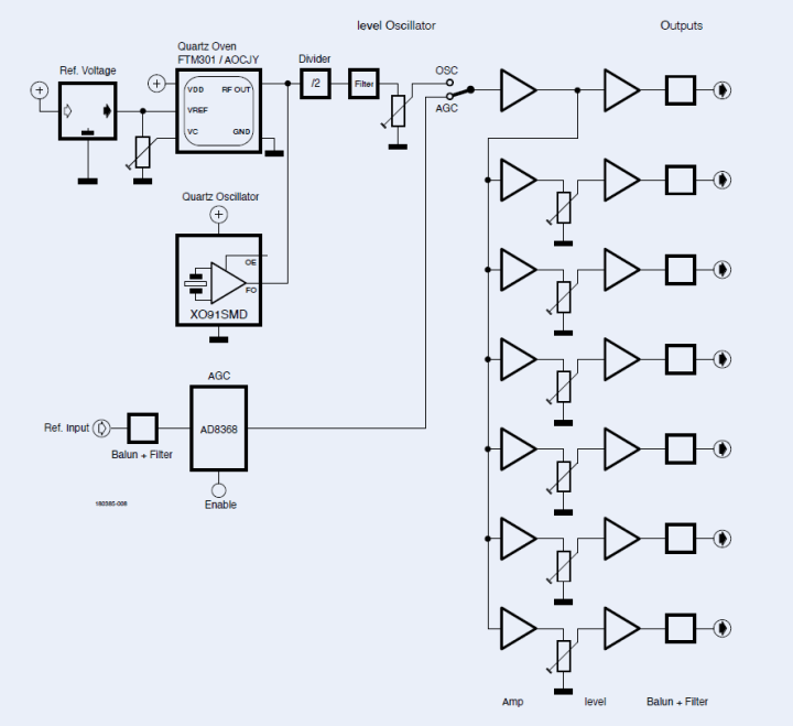
Alternatively, the circuit can also be used simply as a distribution amplifier. If you have a high-quality external reference frequency available, you can feed it into the reference input at the bottom left. After amplitude stabilization by a special RF amplifier (AGC), this signal is fed to the distribution amplifier bank on the right as a reference.
Circuit
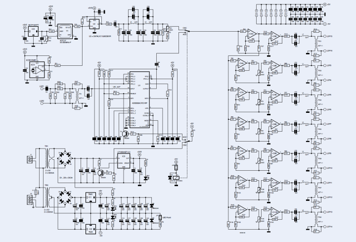
As you can see in the circuit in Figure 2, the digital and analog parts are supplied separately. The clock generation is supplied by the 3.3 V power supply around Tr1 and IC3. The heating of an optional OCXO is also fed from this branch. Its configuration ensures that an accurate and low-drift reference frequency is obtained.
The analog amplifiers are supplied symmetrically with ±5 V from Tr3 and the two classic voltage regulators IC1 and IC2. To ensure clean voltages, a large number of small decoupling electrolytic capacitors, each with 22 µF and 100 nF multilayer capacitors, are distributed across the circuit. The level stabilization of an external reference signal via AGC takes place via the +5 V branch, with small RC filters (R311/C85 and R312/C84) included. Two LEDs on the circuit board indicate that the system is ready for operation. An additional LED can be mounted on the front panel. When all output stages are fitted, a current of around 180 mA flows in the ±5 V branch.
Oscillators
A high-precision, heated quartz generator of type FTM301 from FOX or, for example, type OH300-50503CF-020.0M from Connor-Winfield (Y1 in Figure 2) is used as the oscillator. For lower quality requirements, a simple 20 MHz quartz oscillator (XO1 in Figure 2) is also sufficient. Of course, only one of the two alternatives has to be fitted. If Y1 is fitted, the circuit will draw up to 800 mA from the 3.3 V branch for a few seconds after switching on during heating. The current is then reduced to approx. 350 mA.
The frequency of Y1 can be influenced to a small extent via input VC (pin 1) with a control voltage of 0…2.5 V generated by IC6 and adjustable with R16. If XO1 is fitted instead of Y1, IC6 and the trimming potentiometer R16 can be omitted. Some oscillators contain their own reference voltage, which can be tapped at pin 2. In this case, IC6 can be omitted and R17 can be fitted instead. For oscillators without their own reference voltage, IC6 must be fitted and R17 can be omitted. The reference frequency can be calibrated with R16, which of course requires a suitable and, above all, highly precise external reference frequency.
If absolute accuracy is not very important, the simple and inexpensive XO1 crystal oscillator in an XO91 housing will also do. Once again: Only one oscillator is to be fitted — either Y1 or XO1. Due to the lower current consumption, no extra transformer TR1 is required for XO1 and the rectifier from D1...D4 is also omitted. Instead, R5 is fitted to derive the required 3.3 V from the 5.5 V branch. R11 is fitted when XO1 is used and R18 when Y1 is used.
In order to achieve an optimum duty cycle of 50% of the 10 MHz signal, the 20 MHz of the primary clock generator is divided by a D flip-flop. An alternative is to fit 10 MHz generators, which means that U2 is omitted and its input is connected to the output pin by fitting R13. The 10 MHz signal is then freed from harmonics by a passive fifth-order Cauer low-pass filter around L8 and L9, turning the rectangular signal into a sine wave. The cut-off frequency of the filter is 11 MHz, its ripple is only 0.1 dB, and the input and output impedance is 100 Ω. The voltage divider R14/R15 reduces the input signal, and C22 removes the DC voltage components (= half the operating voltage).
R50, R51, and R52 terminate the output of the filter. The amplitude can be adjusted with trim pot R51 and adapted to the input level range of the AGC. The relay K1 and a switch on the front panel can be used to select between the signal from the internal generator and the reference input.

Distribution Amplifier
IC5A amplifies the signal by a factor of 2 and distributes it to six of the seven output stages via a line terminated with 50 Ω (R130) to avoid reflections on the PCB traces and to achieve as equal a level as possible at all inputs of the seven output stages. The 50 Ω resistor of these stages is used to decouple the input capacitance of the op-amps installed there. Six of these stages are fitted with two video op-amps each. The amplitudes of these six channels can be individually adjusted with their 500 Ω trimpots.
The second op-amp of IC5 drives a serial bandpass filter consisting of the two parallel-connected capacitors C66 and C67 plus the coil L7 and finally the HF transformer Tr51 of type ADT1-1 via a 50 Ω resistor. This output stage has no trimmer potentiometer and its output voltage is therefore not adjustable.
Generally speaking, if you don’t need galvanic isolation, you can leave out the HF transformers Tr51 to Tr57 and fit two 0‑Ω resistors instead. In my prototype, I used MAX4392ESA op-amps in a SOIC8 package. However, you can also use other video amplifiers that are suitable for a power supply of ±5 V. With galvanic isolation and a metal front/rear panel, it is obviously necessary to ensure that the BNC sockets are insulated!
Reference Input and AGC
An AGC IC of type AD8368 from Analog Devices (U1) is used for this subcircuit. The wiring in Figure 2 corresponds to the recommendation in the data sheet. In order not to overdrive the input, an attenuator of 6 dB is connected before the HF input transformer Tr81. If galvanic isolation is not required, the transformer can also be omitted here and replaced by the two resistors R307 and R308. Level stabilization via AGC works with input signals between 70 and 2,000 mVSS at 50 Ω. Lower input levels will reduce the output level — higher input levels will increase it.
Power Supply
After switching on the circuit with a cold OCXO, significantly more current flows than later in the tempered state. For this reason, a relatively powerful transformer with Schottky diodes and a large filter capacitor is provided. The stabilized 3.3 V is generated by the LT1963AET-3.3 low-drop regulator (Analog Devices). The regulator must be cooled. For this purpose, it can be screwed onto the rear wall of an aluminum housing with insulation. Its output voltage can be switched off via the shutdown input if you want to use the external reference frequency and operate the circuit as a distribution amplifier only. This measure prevents interference between the internal generator signal and the external reference signal. Relay K1 is controlled by a switch on the front panel, which is connected to JP2. A changeover contact of the relay selects the input signal for the distribution amplifier. The other contact controls the SHDN input of IC3 via T1 and the ENBL input of the AGC via T2.
One more note on the design: Good thermal insulation of the OCXO will reduce its power consumption. It has reached its maximum accuracy after 30 minutes at the latest.
Fitting Options
As has already become clear, the circuit board provides for several fitting options. The optional components are marked with an asterisk in the parts list. For the sake of clarity, the fitting options are specified here once again:
OCXO or Simple Quartz Generator
For the OCXO Y1, Tr1, the diodes D1…D4, and C1 must be fitted. R5 is omitted. For XO1, Tr1, D1…D4 and C1 are omitted. R5 is fitted instead.
Oscillator with 20 or 10 MHz
For 20 MHz oscillators, the divider U2 must be fitted. R13 is omitted. For 10 MHz oscillators, U2 is omitted. R13 must be fitted.
Reference Voltage of the OCXO
If the OCXO has an internal reference voltage source, IC6 is not required and R17 must be fitted. Without an internal reference voltage source, IC6 is required. R17 should not be fitted in this case.
Internal or External Frequency Generation, or Both
It is possible to equip only the internal oscillators or only the input for an external reference with AGC, or both parts. When using an internal generator, the AGC is switched off. When using the external input with AGC, the 3.3 V power supply and thus the oscillators and the divider are switched off.
Galvanic Isolation
If galvanic isolation is not required, the RF transformers can be omitted. In this case, the two 0 Ω resistors per transformer must be fitted to bridge them. In this case, the correct polarity must be observed when connecting the BNC sockets.
R302 and R305
These resistors are used to achieve an exact resistance value by connecting them in parallel with R301 and R306. The specified values of R301 and R306 are accurate enough for the attenuation of 6 dB envisaged here. R302 and R305 can therefore be omitted.

Construction
Figure 3 shows the partially assembled board, the layout files of which can be downloaded free of charge in Eagle format from the Elektor website. Figure 4 shows a board installed in a plastic case with metal front and back panels. As already mentioned, the BNC sockets should be installed with galvanic isolation. The reference generator described in this article is versatile, very accurate, and avoids ground loops in complex test setups. By the way, some empty boards are still available from the author.

Editor's note: Translated by Jörg Starkmuth. The article, 10 MHz Reference Generator (180385-01), appears in Elektor May/June 2024.
Discussion (0 comments)