
Nano sandwich takes the heat off
September 18, 2018
on
on
Adding an extra encapsulating layer on top of two-dimensional layers used to fabricate nanoelectronic devices significantly reduces the risk of component failure due to overheating.
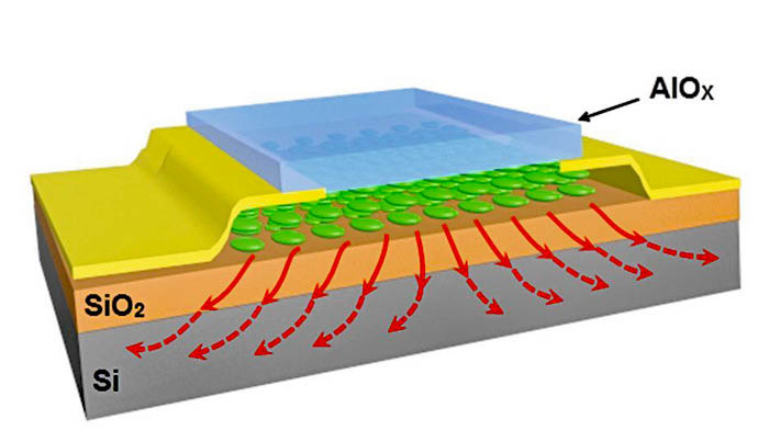
2D materials such as graphene promise a huge potential in the field of semiconductor device manufacture. A layer of the material is just one atom thick allowing components to be significantly smaller than those fabricated using conventional 3D materials. Current research has however highlighted poor thermal conduction between the 2D layers and the device substrate so that as current increases in the device, localized hotspots develop which leads to overheating and device failure.
A team working at the University of Illinois has had some success in overcoming this problem by overlaying the 2D layer with an additional ultrathin material to create a ‘nano-sandwich’. An experimental transistor was fabricated using a silicon oxide substrate, carbon 2D material and aluminum oxide for the encapsulating layer. This additional layer on top of the structure produced a doubling of the thermal energy transfer between the 2D material and the silicon substrate at room temperature.
Researchers from the University of Illinois at Chicago College of Engineering published the results of this study in the Journal Advanced Materials.
Read full article
Hide full article
Discussion (0 comments)