
Quiz time: what’s the biggest threat to IoT?
May 3, 2016
on
on
Okay so the image gave it away: it’s ESD (electrostatic discharge), commonly recognized as the small jolt you get when you get out of a chair and then touch, say, your daughter’s iPhone. That jolt is harmless, but for system designers, ESD provides a threat to the integrity and reliability of “their” piece of the Internet of Things. As the charge spreads out on the surface of the application, some or most of the charge can make its way through the connector (or other interface) and into the sensitive circuitry inside.
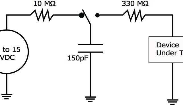
To combat and prevent the effects of ESD you first have to understand the nature of the beast, so let’s model it! The Human Body Model (HBM) is consists of a 100-pF capacitor discharging through a 1.5 MΩ resistor. Test voltages of 500 V to 1,000 V are typically used. This test is performed on integrated circuits. Hell no, says IEC 61000-4-2, you should discharge 150-pF through 330-Ω using 8 kV (contact) to 15 kV (air) as voltage sources. ISO 10605 and DO 160 section 25 use yet other definitions to model the short but disastrous current surge!
Whatever the testing method and ‘resistive’ diversions, the on-chip ESD structures should be able to handle the remaining energy and protect the functional core IC. The Littelfuse ESD Suppression Selection Tool provides a background on counter-ESD’ing by offering a simulation. It takes into account key parameters of the IC as well as those of the intended ESD protection component. Happy sparking!
Read full article
Hide full article
Discussion (3 comments)