What Are PCB Printers, and Have They Reached the Mainstream?
Additive rapid prototyping has changed the world of manufacturers and makers alike. From aircraft parts to plastic housings, 3D printers are seemingly in use everywhere. But what about printing your own circuits? Here we take a look at the world of PCB printers.
Wouldn’t it be great to print a printed circuit board (PCB) just like a document or picture? With just a single mouse click, your design emerges, moments later, as a completed PCB. Well, thanks to a handful of manufacturers, such rapid prototyping PCB printers are available. However, the approaches and equipment are varied.
Currently, PCB manufacturing is a subtractive manufacturing technique. Most PCBs start as copper-clad FR4 material, with the copper being removed to leave the desired electrical interconnections between the circuit’s components. According to some estimates, the market for PCBs is huge ($76 billion by 2027) and dominated by manufacturers in Taiwan and China who, combined, have a market share of more than 60%.
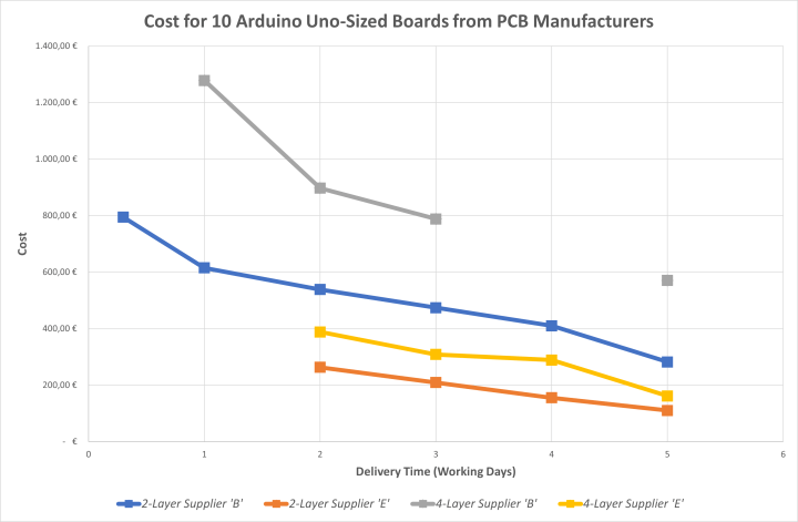
The challenge for most makers and businesses are delays during the prototyping phase of their electronic circuits. The cheapest PCB manufacturing costs have the longest delivery times. This means that whenever a mistake is found in the design, your next batch of corrected PCBs take a week to arrive. Then you have to add the time to place and solder the components. Shorter turnaround times of as little as eight hours are possible but cost around six times as much for the same order.
Rapid turnaround time for PCBs can cost six times more than a five working days delivery time order. (Correct as of January 2021)
PCB Printers: Ink Dispensing Approach
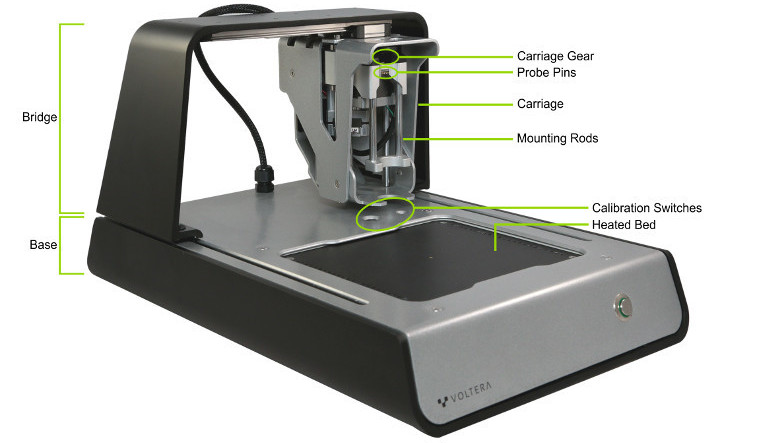
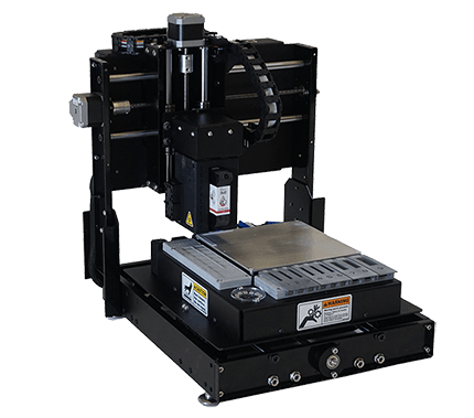
One PCB printer product, the Voltera V-One, uses an X-Y plotter design to dispense conductive ink to a substrate. Once applied, the substrate and ink are heated using an integrated heating element to cure the ink. Like a regular printer, the V-One connects to a host computer via a USB cable, and the associated app guides the user through the manufacturing process.
The Voltera V-One is build like an X-Y plotter and dispenses conductive ink and solder paste from syringes. (Source: Voltera)
Conductive ink is dispensed from a syringe, much like the solder paste used for hand dispensing. The minimum attainable track width is defined by the nozzle used, with this particular printer achieving a track widths down to 0.2 mm or 8 mil. That’s enough for 0402 (imperial) passives or ICs with a minimum pin-to-pin pitch of 0.65 mm/26 mil. For the substrate, FR-4 or FR-1 board can be used (obviously not copper plated).
An Alternative Metal for PCB Traces
Unlike a traditional PCB with copper tracks, the conductive ink is primarily made of silver mixed with ‘the vehicle’, namely the binders, solvents, additives, and dispersants that help the ink flow and dry during application. Because of this, the conductivity of the tracks is lower than an equivalent copper-based PCB. For example, 35 μm (1 oz) copper-clad FR-4 has a 0.5 mΩ/square resistivity. Silver-based conductive inks come in at around 12 to 40 mΩ/square, depending on the manufacturer. For most applications, the implications are minimal, and most analog and digital circuits can be tackled without issue.
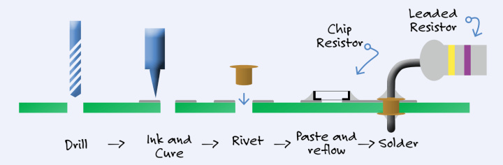
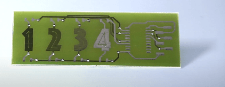
Once your PCB has been printed and cured, the same printer can drill the holes for through-hole components, apply solder paste, and solder the components in place. The user is only required to insert the correct drill bit in the chuck and hand-place the surface mount components.
The PCB printer manufacturing process used by the V-One.
Double-sided PCBs are also possible by printing tracks on both sides of the FR-4 substrate. Through-hole vias are implemented by drilling the holes and then fitting copper rivets. These are also useful as the attachment point for soldering through-hole components.
PCB Printers: Inkjet Approach
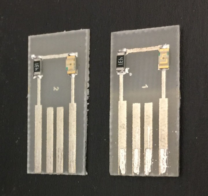
Another approach makes use of the same technology used in inkjet printers. This is the solution used by the BotFactory SV2. The printer supports different substrates upon which the conductive ink is ‘jetted’ before curing using a heater integrated into the printing bed. To support multi-layer PCB designs, the SV2 uses a second printer cartridge that contains an insulator. This is printed over the conductive tracks, enabling the construction of up to four-layer PCBs. Each insulator layer is cured using an in-built ultraviolet light.
The BotFactory SV2 PCB printer can also perform pick-and-place. (Source: BotFactory)
The result is a very thin multi-layer PCB printed on a single side of the substrate used. Through-hole components can be supported using copper rivets, providing the chosen substrate, such as FR-4, is thick enough for the mechanical fixture. However, rivets aren’t required for vias. Instead, the conductive layers connect through gaps in the insulating layer. Additionally, the SV2 is particularly suited to developing flexible circuits because of the thin layers attained with the inkjet printing approach. Users have reported success using substrates of Kapton tape and even fabric.
A four-layer PCB printed using the BotFactory SV2. An insulation layer is printed and cured between each conductive layer. (Source: BotFactory)
Another feature of the SV2 is its pick-and-place (P&P) function. After applying solder paste to the pads, the P&P head can collect a range of surface mount components prepared in slots around the edges of the printing bed. Once placed, the heated bed melts the solder paste. This enables the highly-automated manufacturing of small quantities of prototype PCBs.
Advantages and Disadvantages of PCB Printers
Perhaps the first point to make is that the PCBs these printers create are unlike classic PCBs. The critical difference is the properties of the tracks due to the use of silver rather than copper. Any hand soldering requires a Tin-Bismuth-Silver solder and a maximum solder tip temperature of 180°C. Higher temperatures risk destroying the tracks, although the use of copper rivets reduces this risk when soldering through-hole components.
Another challenge is component heat dissipation. The copper of a traditional FR-4 PCB can be relied upon to dissipate a certain amount of heat from, for example, power devices. With these silver-based designs, you may need to be a little more creative. Thanks to the SV2’s ability to print on a wide range of substrates, users have had success printing onto heatsinking materials. By printing an insulation layer before applying the conductive tracks, even copper-clad FR-4 can be used as the base material.
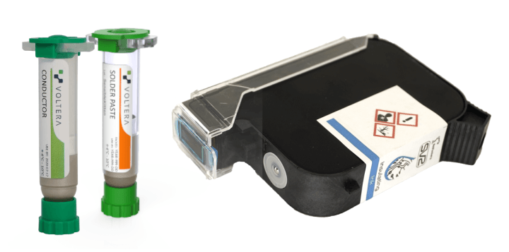
Conductive inks and solder pastes for PCB printers. (Source: Voltera [left] and BotFactory [right])
Perhaps the biggest challenge to using PCB printers is caring for the consumables. The inks and solder pastes have a shelf life of between 6 and 12 months. However, care must be taken to refrigerate them after use, otherwise, they solidify and become unusable.
On the positive side, PCB printers offer users competent rapid prototyping of circuits, especially when trialing alternative, flexible substrates. Users have also had success with RF designs, such as a 915 MHz filter and circuits operating at up to 6 GHz. And tests have shown the tracks to be quite durable. Using a printed board to implement a USB connector, one board survived over 10,000 insertion cycles.
This USB connector created by BotFactory's SV2 survived 100,000 insertions. (Source: BotFactory)
The Future for Manufacturing?
In the domain of prototyping and education, PCB printers definitely have their uses. Suppose your organization develops a lot of new circuit boards every year. In that case, the rapid turnaround for board iterations, along with the small manufacturing-run support with component P&P head options, could prove to be a good investment. These printers also make the electronics manufacturing process more transparent to students at schools, colleges, and universities.
However, the additive manufacturing process used by these printers is not really suited to mass board manufacture. There are, however, others who are looking to change the face of PCB manufacture. The winner of the productronica 2021 Fast Forward Award, ioTech from Israel, has an additive manufacturing concept based upon Continuous Laser-Assisted Deposition (CLAD). This promising technology not only offers the manufacturing of multi-layer circuit boards in minutes, but it could also enable circuits to be constructed in ways impossible with current processes, leading to innovation in wearable tech and implantable medical technology.
Finally, if you’d like to learn more about the PCB printers mentioned here, take a look at Elektor’s “Buyer’s Guide to PCB Printers.”
Elektor Magazine has been one of the leading sources of information on electronics for engineers, designers, start-ups and companies for 65 years. Our magazine is powered by an active community of electronics engineers – from students to professionals – who are passionate about designing and sharing innovative ideas.
For them, we publish hundreds of items a year, in formats such as articles, videos, webinars, and other learning formats. Our mission is to share knowledge in every possible way and inspire readers with the latest developments within the electrical engineering sector.
Thank you for your vote!
Leave further comments in the fields below.
Thank you for your vote!
If you wish to leave a comment with your rating, please first use the login below. If not, just close this window.

Discussion (3 comments)