Voltera V-One, a Desktop Prototyping Tool for Custom PCBs
If only hardware development was as fast paced as software development, just imagine how many more physical products could be contributing to the rise of our global economy! Good news: great strides can be made by prototyping PCBs right on the desktop and guess what, a machine to do just that is now available.
If only hardware development was as fast paced as software development, just imagine how many more physical products could be contributing to the rise of our global economy! Good news: great strides can be made by prototyping PCBs right on the desktop and guess what, a machine to do just that is now available.
Printed Circuit Board (PCB) prototyping is the leading factor limiting the hardware development cycle. Before mass manufacturing, PCB designs are usually fabbed in gradually increasing volumes as the design is refined. Currently, hardware developers are either fabricating their designs in-house, which is a jarring do-it-yourself method utilizing corrosive chemicals, or more commonly, outsourcing to overseas factories that charge large minimum order quantity (MOQ) fees and have several-week long lead times. With each iteration, money is lost and time is wasted, drastically hampering the product’s progress and innovation as a whole.
High-tech regions like Silicon Valley have created an infrastructure to mitigate this problem, by creating turnkey services for PCB turnarounds within three to four days. This leaves designers with the uncomfortable choice between these very expensive solutions or the usual painful and slow development cycle to bring their ideas to market.
Hardware developers need a better way to prototype PCBs, so that they can cut down their development time, save money, and get their products to market faster.
Conventional prototyping methods aren’t cutting it
Presently, mainstream PCB patterning is largely a subtractive process. In order to produce conductive patterns, this process employs chemical etching whereby conductive material is removed from a single side, or both sides of a copper-clad base material.
Hardware developers rely on these chemical etching processes to prototype PCBs either in-house, or typically by outsourcing the process to factories — usually in China. Although chemical etching is by far the most commonly used subtractive process for PCB fabrication, the overall process is time consuming, costly, and dangerous. In addition it causes enormous waste and chemical by-products that are harmful to humans and the environment. Appallingly, 2 million tonnes of PCB by-product has been produced since 1929, some of which still remains in the environment today.
Other subtractive methods have been developed in an attempt to solve this issue with the delayed hardware development cycle. Isolation routing, for example, uses a computer guided drill bit to remove unwanted copper from a copper-clad base material. With lower setup required and faster production times, this subtractive milling process is targeted towards in-house prototyping. However, this process is far from ideal and has several drawbacks. For one, it is limited to rigid substrates and can only produce single or double sided boards. In addition, routing of the copper-clad base produces fibreglass dust particles that are harmful to the user.
A unique additive approach
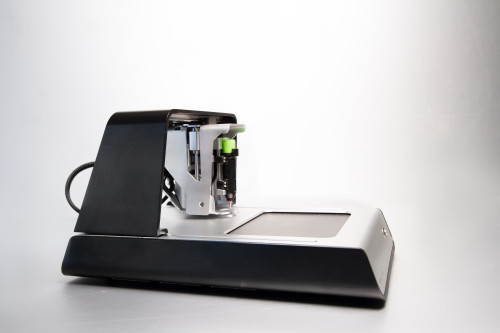
Recently, additive processes for fabricating circuit boards have drawn much attention in the field of rapid prototyping. Since material is added and not removed, there is little to no waste. Additionally, the equipment for this application can be small enough to fit on a benchtop, rather than the full factory required by traditional processes. As pioneers in this industry, Voltera recognized the advantages that this additive approach can provide to early-stage hardware development and created the award-winning Voltera V-One: a desktop prototyping tool for custom PCBs.
How it works
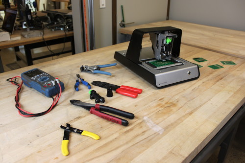
The Voltera V-One is a multifunctional tool that allows hardware developers to prototype PCBs within an hour. This new tool creates functional electronics quickly and cost-effectively, allowing developers to build PCBs on site for tens of dollars, instead of outsourcing their designs or utilizing harmful subtractive processes for hundreds or thousands of dollars. The V-One’s feature set includes capabilities that allow the user to:
dispense silver conductive ink to print circuitry onto the standard FR-4 substrate and a variety of other materials;
dispense solder paste onto both V-One printed and traditionally fabricated boards;
reflow solder components directly on the built-in heated platform.
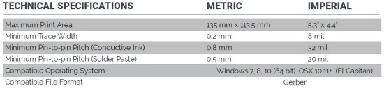
Starting with 20 µm precision
The V-One accepts Gerber files, so the developer can design their PCB in any CAD software they prefer (Altium, CadSoft EAGLE, PADs, OrCAD, KiCad, etc.). Before the print, a detachable touch probe sensor is utilized to generate a topographical map of the printing surface, down to 20 µm precision. This grid of points stores information about the height difference between the substrate and the nozzle tip, which is critical for accurate printing. Dispensing the conductive ink at a consistent height from the printing surface ensures the geometry of the traces matches their definitions in the design files.
Printing with silver nanoparticles
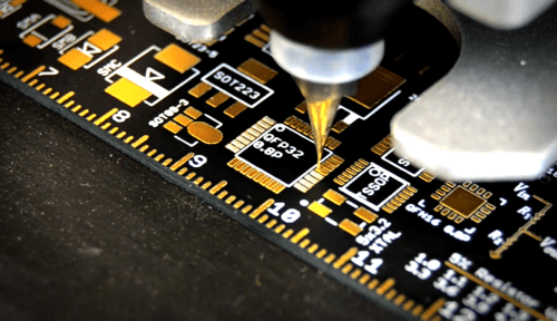
Once a height map of the surface is established, the touch probe can be removed and interchanged with the dispensing mechanism. This mechanism utilizes a piston to extrude the highly specialized silver nanoparticle ink out of a precision-machined 200-µm nozzle.
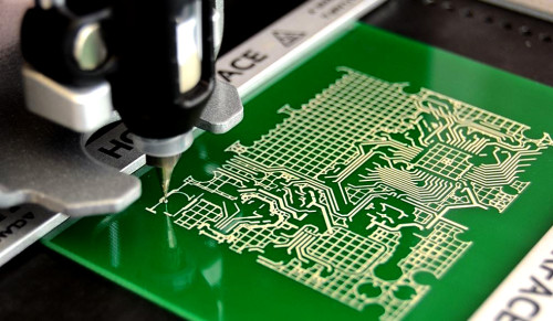
Figure 1: V-One printing a circuit with conductive ink
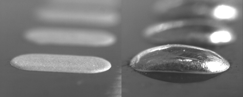
After uploading the Gerber files, conductive ink is laid down as the traces and pads making up the PCB pattern (Figure 1). Next, the V-One’s integrated 550-watt heater thermally cures the ink during a 20-minute bake cycle. During this process, solvents are evaporated and polymerization is initiated, fusing the silver nanoparticles into a tight silver matrix. What remains are the silver traces that are fully conductive and solderable (Figure 2).
Figure 2: Microscopic view of silver nanoparticle printed pad before (left) and after soldering (right)
Finishing with solder paste dispensing and reflow
After printing, the V-One can dispense solder paste onto pads, and reflow the components with the integrated reflow platform. These features are compatible with boards printed by the V-One and with traditionally fabricated boards, thus eliminating the frustrations associated with multiple stencil iterations, and saving huge costs and time on the even more exorbitant assembly process.
The additive approach of depositing solder paste directly where it is required means it is not wasted through the incredibly tedious stencil based screen printing processes. Pad alignment for paste dispensing is accomplished using the touch probe sensor. Using two user-selected pads or fiducials, the touch probe will interpolate the location of the remaining pads in XYZ space. This alignment technique can also be used to print onto boards with pre-existing features such as recessed areas. The dispensing operation is shown in Figure 3.
Figure 3: V-One dispensing solder paste on pre-fabricated PCB
Potentially boundless prototyping
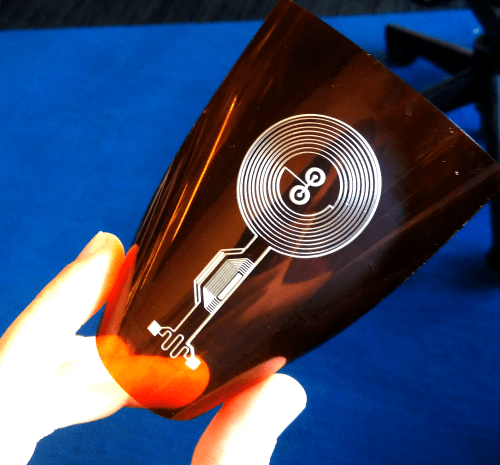
A refreshing additive approach to PCB manufacturing allows for experimental prototyping that was not possible before. Electronic prototyping is no longer limited to circuitry on conventional, rigid FR-4, but is now versatile to an abundance of materials such as Polyimide and PET, glass and silicon, bio-compatible thin films, consequently allowing for accelerated research efforts in fields of flexible electronics, radio frequency applications (Figure 4), and medical diagnostics devices, respectfully. Such an approach is bringing prototyping back to the hands of the creator and is truly a catalyst for innovation.
Figure 4: Flexible antenna printed on Kapton
Small to medium businesses are able realize their products faster than before, hence exercising their truly unique advantage over the often lumbering corporate sector: speed and agility. Although focused primarily on these applications, the tool has also lowered electronics’ barrier to entry enough that it has been used by university students in educational projects and even by parents introducing their young children to the joys and challenges of making.
From Voltera’s headquarters in Canada the team has been shipping globally, starting with the Americas and expanding to fulfill orders all over Asia, Africa, Oceania, and Europe. Their vision stands to modernize manufacturing and make hardware development painless for anyone prototyping in workshops, offices, laboratories, or classrooms.
Read full article
Hide full article
About Katarina Ilic
Katarina Ilic is a Nanotechnology Engineer who specializes in the development of nano-functional materials for various applications. In 2013 she co-founded Voltera Inc., which aims to disrupt hardware innovation through additive manufacturing. The young compan... >>
Add a rating to this article
★★★★★
★★★★★
Page 1 / 1
Login
No account yet?Register for free!
Forgot password?
Please enter your email address. Instructions for resetting the password will be emailed to you now.


Discussion (1 comment)