
2-D nanowires make transparent components
December 13, 2017
on
on
According to an MIT News article, electronic components can now be made so thin with the help of 2D nanowires they ultimately become transparent. The next revolution in electronics is likely to be based on the development of flat, almost two-dimensional, semiconductors which, like graphene, are only a few atomic layers thick.
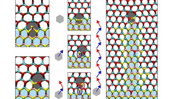
The nanowires have been produced using a technique developed by researchers in Saudi Arabia at King Abdullah University. The wires are made by depositing a layer of molybdenum disulfide alongside tungsten diselenide. Both materials have semiconductor properties which makes them suitable as base materials for electronic components. Researchers at Cornell University modified the technique so that they were able to induce long straight wires of molybdenum disulfide only a few atoms in diameter which extend into the tungsten disulfide. MIT researchers working together with colleagues from the Taiwan national research academy and Texas Tech University have produced a computer model of the mechanism which underlies the formation of these nanowires.
According to Gang Seob Jung (MIT graduate student in civil and environmental engineering and co-author on the paper) they will go on to investigate the suitability of this material for use in solar cells and for applications using sunlight to split water. He went on to say that all the interesting processes take place at the interface, when you have many nanowire interfaces there is the potential to improve solar cell efficiency. The future for 2-D materials is thought to be so great that they could eventually replace nanoscale silicon.
Read full article
Hide full article
Discussion (0 comments)