
Measuring Power Inductors
on
Most LCR meters measure components with a current of just a few milliamps. For capacitors and resistors this is fine, but the inductance (and properties in general) of power inductors vary with the (DC) current level. To test this influence of the current on inductance, all that is needed is a series (current sense) resistor with very low resistance and a stable power supply with high output current. This principle has been applied in many different ways over the years. A power switch (often a MOSFET) and pulse generator is needed to switch off the voltage across the inductor before it gets too high. An oscilloscope is used to monitor the current through the inductor. This circuit is stand-alone. The maximum current is adjustable and a trigger signal for the oscilloscope is also provided. No external pulse generator is needed. A PCB ensures that resistance between power supply, inductor, MOSFET and current sense resistor is minimal.
Circuit
In the schematic shown in Figure 1, two timers from a CMOS 4538 are used. The timing of a 4538 is set by the RC constant (in this case R8/C3, R9/C4). For IC2A this means 1 µF * 1 MΩ = 1 s. IC2A activates the MOSFET T3 once every second. The second timer is used to limit the time the MOSFET is conducting to 1 ms. If a longer maximum pulse is needed, the value of R9 must be increased accordingly. With this very short duty cycle, no heatsink is needed for T3 and D3. A fast Rail-to-Rail I/O opamp (IC1) of type AD8032 is used to monitor the current through the 10 mΩ current sense resistor R4. It serves as a comparator, and if the voltage level across R4 is higher than the level set with P1, the output of IC1A becomes low and resets IC2B, the MOSFET is switched off. At the same time IC2A is triggered, output Q (pin 6) becomes high and provides a trigger signal for the oscilloscope on K2. After one second, /Q switches to high level and triggers IC2B, and T3 switches on for the next measurement cycle. The current through the inductor starts to rise and the process is repeated.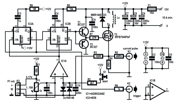
The two timers are configured in non-retriggerable mode. Output Q of IC2A is connected to its +TR input, and /Q of IC2B to its -TR input to prevent glitches that would extend the pulses. C10 is added to extend the reset pulse of IC2B, but most of all the trigger pulse of IC2A. The latter input level needs to be lower than the reset pulse to activate triggering. At a low current setting (P1) — without C10 — the output of IC1A would not get low enough to trigger IC2A. If there’s no trigger pulse at power-up, push button S1 is used to start the measurement. T1 and T2 are used to turn T3 faster on and off. The gate current and the parasitic capacitance of inductor under test cause a spike across R4. This doesn’t influence the measurement.
Example
As an example, a power inductor from Murata Power Solutions was tested, type 1433445C, 330 µH, specified for a maximum DC current of 4.5 A. The datasheet only mentions for all inductors in the series that the specified maximum DC current occurs where inductance drops to 60% or at a temperature rise of 50°C, whichever is sooner. Looking at the measurement in Figure 2, it can be seen that saturation of the core sets in at about 10 A. This is interesting to know about this inductor or any other. This means it can be used in applications with slow repeating large current pulses up to 10 A with no loss of inductance. But always be sure the DC current through the inductor is never higher than the value specified in the datasheet! The circuit is designed for a little over 15 A.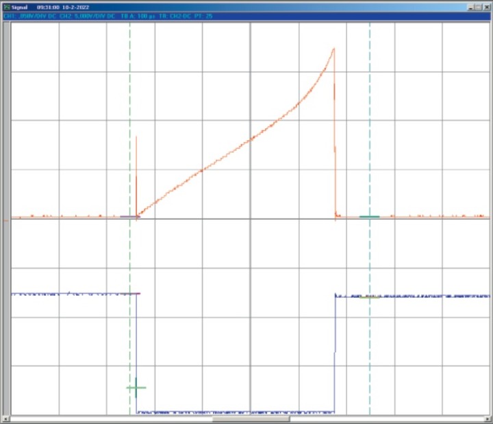
Best is to use a power supply with this maximum current to be sure the voltage doesn’t drop; it would affect the accuracy of the measurement. But, the power supply is decoupled with three capacitors with very low ESR (C7/C8/C9), just to make sure. In practice the use of a power supply with less out current is of course an option; you decide. A 15 A fast fuse is added for safety in the event the MOSFET short-circuits. A disadvantage is an extra voltage drop across the fuse. Most power inductors are in the range of a few 100 µH, and the duration of the peak current is very short. Use thick wires to connect the Lx and 12 V terminals on the PCB to the inductor under-test and the power supply, respectively. Alternatively, two wires in parallel can be connected to the two 1.4 mm holes in the footprints on the PCB.
In the scope picture, the red trace is the current through the inductor with 5 A/div, and the blue trace is the signal at the trigger output. The glitch at the start is caused by switching on the MOSFET and is partly due to charging the gate capacitance and partly the parasitic capacitance of the inductor.
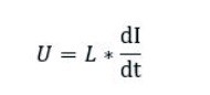
The standard formula for the voltage across an inductor can be used to calculate the time it takes for the current to reach the value set by P1:
Rearranging the formula:
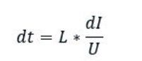
When a power inductor is connected to a 12 V power supply, the current will increase linearly over time, as long as the core doesn’t saturate. The time to reach 10 A current through a 330 µH inductor would be 275 µs. But we can also calculate the real inductance from the time shown on the oscilloscope when 10 A is reached (290 µs). The inductance is U*dt/dI, so 348 µH.
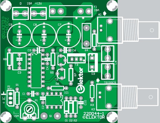
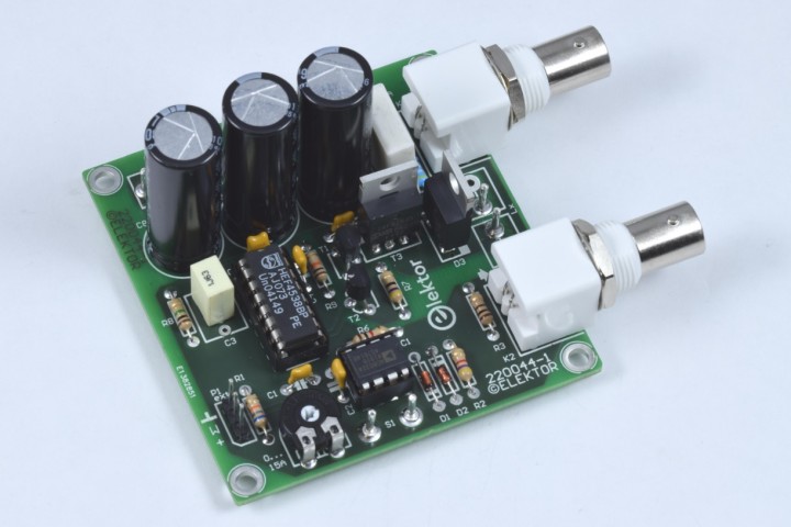
PCB
For this project, a PCB was designed; its Gerber files can be downloaded here. While keeping dimensions of the PCB in Figure 3 small, some connections are routed parallel on both sides of the PCB to keep the resistance of the measuring loop as low as possible. The MOSFET used is a IRFB7545PBF in TO-220 case, with RDS(on) about 5 mΩ. Total resistance of MOSFET and current sense resistor is about 15 mΩ and at 15 A the voltage drop is 0.23 V, when copper losses of the PCB traces and connecting wires are not taken into account. The flyback diode to suppress the voltage spike when the MOSFET is turned off is a MBR1645 which can handle an average current of 16 A and a 45 V reverse voltage. The maximum power supply voltage for the op-amp is 12 V, and this is also the maximum voltage for this circuit. Even though the maximum current through the inductor under test is high, the average supply current is only a few milliamps.Questions About Measuring Power Inductors?
Do you have any technical questions or comments power inductors or any of the topics mentioned in this article? Contact the author at Ton.Giesberts@elektor.com or the Elektor team at editor@elektor.com.
Editor's note: THis article originally appeared in Elektor Summer Circuits 2022.
Measuring Power Inductors: Components
Resistors
R1 = 68 kΩ, 0.25 W, 5 %
R2 = 4k7, 0.25 W, 5 %
R3 = 100 Ω, 0.25 W, 5 %
R4 = 0.01 Ω, 5 W, 10 %, radial low induction, pitch 9 mm (Fukushima Futaba MPC75)
R5 = 49.9 Ω, 0.25 W, 1 %
R6 = 1 kΩ, 0.25 W, 5 %
R7 = 47 Ω, 0.25 W, 5 %
R8 = 1 MΩ, 0.25 W, 5 %
R9 = 10 kΩ, 0.25 W, 5 %
P1 = 1 kΩ, trimmer, top adjust (Piher PT10LV10-102A2020-S)
Capacitors
C1,C2,C4,C5,C6 = 100 nF, 50 V, X7R, 5.08 mm pitch
C3 = 1 µF, 63 V, PET, 5/7.5 mm pitch
C7,C8,C9 = 3300 µF, 16 V, diam. 12.5 mm, 5 mm pitch, 3.4 A, 15 mΩ (Rubycon 16ZL3300MEFC12.5X35)
C10 = 220 nF, 63 V, PET 5 mm pitch
Semiconductors
D1,D2 = 1N4148, DO-35
D3 = MBR1645, TO-220 2 pins
T1 = BC337, 800 mA, TO-92
T2 = BC327, 800 mA, TO-92
T3 = IRFB7545PbF, 4.9 mΩ, 95 A, 60 V, TO-220
IC1 = AD8032ANZ, DIP-8
IC2 = 4538, DIP-16
Others
K1,K2 = BNC connector, PCB mount, right angle, jack, 50 Ω
K3 = Pin header, 3x1, vertical, 2.54 mm pitch
F1 = 2 fuse clips, 20 A, Littelfuse 01000020Z, for 5x20mm
F1 = cartridge fuse 5 x 20 mm, 15 A, fast acting
S1 = push button, SPST, momentary on
S1,Lx,power supply = 10 x Press Mount Terminal, 1.3 mm (Ettinger 13.14.419)
1 x 8-pin DIP-socket for IC1
1 x 16-pin DIP-socket for IC2
Discussion (0 comments)