
Review: Eurocircuits’ PCB Solver
May 25, 2017
on
on
What Is the PCB Solver?
The Printed Circuit Board (PCB) pooling and manufacturing company Eurocircuits offers a free online tool suite — PCB Visualizer — that enables clients to check their PCB designs for manufacturability before ordering. Not only allow these tools to visualize how a board’s production files are interpreted by the manufacturer, they can also highlight problems that for some reason went unnoticed so far. In previous articles we looked at the PCB Configurator and the PCB Checker, now it is time to check out the PCB Solver.What Can You Do With the PCB Solver?
Although it is easy to imagine that for a board manufacturer it is important to know the correct outline of a board, surprisingly many PCB designers forget to include a well-defined outline in their production files. In such cases the people and tools at Eurocircuits try to reconstruct the outline from the available data, but this is not always possible. To avoid incorrect interpretation with possibly unexpected results it is better to include the client in the loop. PCB Solver was developed to do just that.
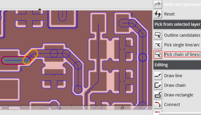
The PCB Solver is a repair tool that lets the client fix some issues like annular ring (AR) and board outline problems flagged by the analyzer tools without having to go back to the CAD package to correct them and then to go through the re-upload process again. For this the PCB Solver features an online board outline and milling editor. The annular-ring-repair-part of the PCB Solver is actually integrated in the PCB Configurator as a simple checkbox.
Test Driving the PCB Solver
A suitable board outline is defined by Eurocircuits as a closed polygon that surrounds all functional copper (copper with pads or drill holes) without being much wider than the functional copper. Such a polygon can live on any layer or even on several layers, as long as they are all identical. If there are more than one candidate for an outline, the Visualizer will flag this.
For this review I modified the Elektor Uno R4 PCB design to create a few outline issues. After adding it to my shopping cart (by clicking the ‘Analyse Data’ button), the PCB Visualizer flags it with a blue exclamation mark. Clicking the PCB Visualizer link opens a new window where my board is shown as a rectangle instead of Arduino shaped. Also I see two warnings, one on the left under ‘Customer Data’ and one on the right under ‘Remarks’, both telling me that no outline was detected. Clicking the ‘Outline’ button on the right opens the ‘Outline/Milling editor’. Now the fun starts.
Read full article
Hide full article
Discussion (0 comments)