
Speedy PCB production using an inkjet printer!
June 1, 2016
on
on
Rapid PCB production for prototype circuits is an old theme. A copper-clad board with a photosensitive mask and an etching bath of caustic chemicals is messy, time-consuming and really yesterday’s technology. Use a specialist PCB production facility and you’re looking at a few days turnaround time, a milling machine will do the job quicker but you need the equipment to start off with. 3D printing conductive tracks has been achieved but the technology is still not main-stream. How about 2D printing direct from an ink-jet printer?
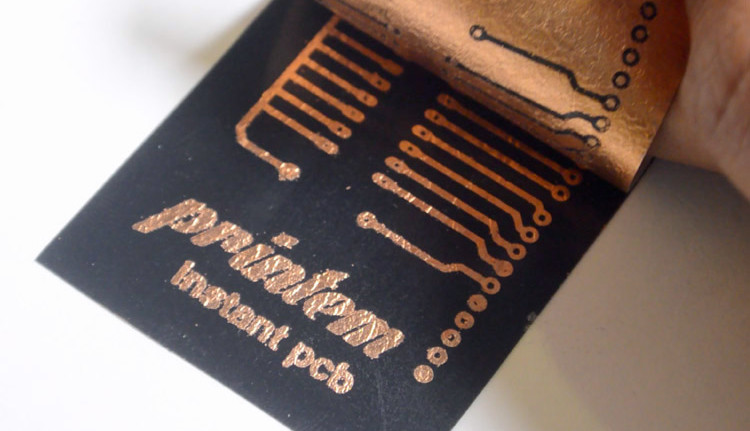
Well the answer to that one is yes! PHD student Varun Perumal Chadalavada at the University of Toronto has developed an amazingly simple technique which can be used with commercial inkjet printers to ‘print’ a prototype PCB. It has been likened to the instant ‘Polaroid’ land film process where an image is impressed on a complex chemical layer and you need to wait a while until the image appears.
The technique prints the PCB pattern onto a sheet of Printem film which is then exposed to light for around 30 seconds and then the top layer is peeled back to reveal the PCB, that’s it!
The processing speed is just about unbeatable. It would be ideal for any lab or workshop when you just want to knock up a quick prototype. A spin-off company has been formed in order to explore the potential market for the product. Technical specs such as track thickness, stability of the product, its durability and solderability and production costs are not yet finalized but from the video above, the process looks very promising.
Read full article
Hide full article
Discussion (1 comment)