
PCBWay’s extended businesses in the PCB industry
March 24, 2020
on
on
Due to technical requirements and differences in manufacturing capabilities, special plates such as Rogers, copper substrates, aluminum substrates, and high-frequency high-speed HDI, special inks, blind buried holes and other special processes PCB factories are either technically incapable or unable to do so. They are either cumbersome to manufacture, high in cost, long in cycle, and have a low number of production, which makes them reluctant to do it or do it less often. As a PCB innovation company, PCBWay is committed to solving the pain points of PCB procurement and meeting customers' various PCB procurement needs.
PCBWay can do 1 ~ 8 layers; the board thickness is less than 3.0mm; the thermal conductivity is 1 ~ 3W; double-sided mixed pressure (FR4 + AL).
Copper substrate is the more expensive one among metal substrates. Its thermal conductivity is many times better than that of aluminum substrates. It is suitable for high-frequency circuits and areas with large changes in high and low temperatures, as well as in the heat dissipation and architectural decoration industries of precision communication equipment.
At present, PCBWay can perform impedance control by using plates made of FR-4, FPC, soft and hard, etc .; the number of layers that can be achieved is 2-20 layers; and the impedance tolerance is ± 10% (limit ± 8%).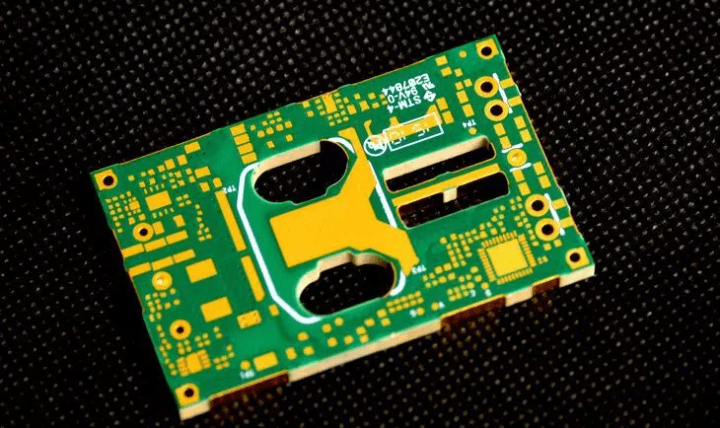
At present, the Rogers sheet used by PCBWay is a ceramic substrate, which can achieve 4-6 layers of pure ceramic pressing; 4-8 layers of mixed pressing.
Get an instant quote here
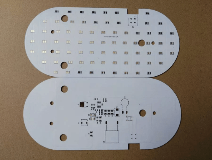
1. Single-sided aluminum substrate
Aluminum substrate is a metal-based copper clad laminate with good heat dissipation function, and it is the basic material of high-power power electronic circuit structure technology and interconnection technology. Generally, a single panel is composed of three layers, which are a circuit layer (copper foil), an insulating layer, and a metal base layer. Double-sided board with structure of circuit layer, insulation layer, aluminum base, insulation layer and circuit layer.PCBWay can do 1 ~ 8 layers; the board thickness is less than 3.0mm; the thermal conductivity is 1 ~ 3W; double-sided mixed pressure (FR4 + AL).
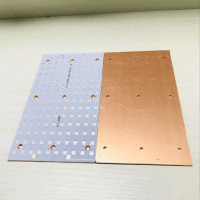 2. Single-sided copper substrate
Copper substrate is the more expensive one among metal substrates. Its thermal conductivity is many times better than that of aluminum substrates. It is suitable for high-frequency circuits and areas with large changes in high and low temperatures, as well as in the heat dissipation and architectural decoration industries of precision communication equipment.3. Impedance control
In the transmission signal lines of electronic devices, the resistance encountered when their high-frequency signals or electromagnetic waves propagate is called characteristic impedance. When the digital signal is transmitted on the board, the characteristic impedance value of the PCB must match the electronic impedance of the head and tail components; once it does not match, the transmitted signal energy will be reflected, scattered, attenuated or delayed, which seriously affects the signal integrity. In this case, impedance control must be performed to match the characteristic impedance value of the PCB to the component.At present, PCBWay can perform impedance control by using plates made of FR-4, FPC, soft and hard, etc .; the number of layers that can be achieved is 2-20 layers; and the impedance tolerance is ± 10% (limit ± 8%).
4. HDI blind buried hole
Blind holes are only visible on one of the top or bottom layers, that is, blind holes are drilled from the surface, but do not drill through all layers; buried holes refer to inner-layer vias, both above and below the hole In the inner layer of the board, in other words, it is buried inside the board. The application of blind holes and buried holes greatly reduces the size and quality of HDI (High Density Interconnect) PCBs, reduces the number of layers, improves electromagnetic compatibility, increases the characteristics of electronic products, reduces costs, and also makes design work easier and faster.5. Rogers
Rogers is a high-frequency plate with excellent dielectric constant and temperature stability. The thermal expansion coefficient of the dielectric constant is very consistent with that of copper foil. It can be used to improve the shortage of PTFE substrate; it is very suitable for high-speed design and commercial microwave. And RF applications. Due to its extremely low water absorption, it can be used as an ideal choice for high humidity environment applications, providing customers with the highest quality materials and related resources in the high-frequency board industry, and fundamentally controlling product quality.At present, the Rogers sheet used by PCBWay is a ceramic substrate, which can achieve 4-6 layers of pure ceramic pressing; 4-8 layers of mixed pressing.
6. FPC
PCBWay can do 1-8 layers; the board thickness is 0.06 ~ 0.4mm; the minimum line width / distance of single and double layers is 2mil, the minimum line width / distance of multiple layers is 3mil; and the copper thickness is 0.33 ~ 2oz.
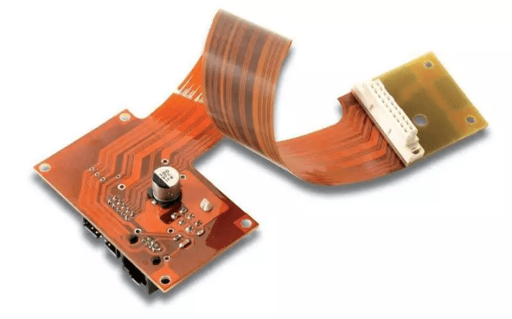
7. Combination of rigid and flexible
The combination of the flexible board and the hard board is to combine a thin layer of flexible bottom layer and a rigid bottom layer, and then laminate into a single component to form a circuit board that is flexible and foldable. Due to the mixed use of multiple materials and multiple manufacturing steps, the processing time of the rigid-flex combination board is longer and the manufacturing cost is higher.Get an instant quote here
Read full article
Hide full article
Discussion (0 comments)