
World record: 5 nm GAAFET IC from IBM, Samsung & GlobalFoundries
June 8, 2017
on
on
A research partnership comprising IBM, Samsung and GlobalFoundries have developed an industry-first process to build silicon nanosheet transistors that will eventually enable production of 5 nm chips. The 5 nm IBM chip is also one of the first ICs based on GAA (Gate-All-Around) topology transistors and also probably the first serious application of EUV (Extreme UltraViolet) lithography.
GAAFETs represent the next evolutionary step after the tri-gate FinFETs with a structure width of 22 and 14 nm. This technique however is only scalable down to 7 nm. In comparison GAAFETs are expected to be able to realize 3 nm structures. Who said Moore's Law was already on the ropes?
To date, the transistors have been fabricated by stacking different materials on ICs. With ever-decreasing structure size however, it becomes increasingly difficult to produce such 2D transistors with good properties (switching speed and leakage currents). Fewer atoms are available to take part in the electrical flow.
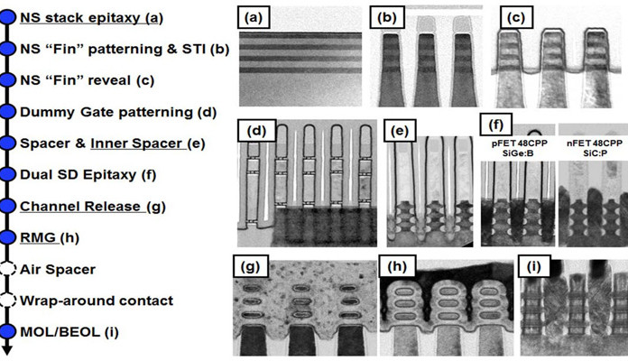
FinFETs solved this problem by making use of the third dimension. A 3D-fin protrudes from the substrate and thus contains more atoms. The resulting structure is narrow, allowing many transistors to be accommodated. GAAFETs, however, are almost 2D layered-structures again, but constructed with the benefit of 3D topology. The type used here are a kind of flipped FinFET, where the fins are no longer perpendicular to the substrate but lie flat. A fin can be viewed as a kind of nano-wire or nano-layer extending between drain and source. With IBM's GAAFET, three such layers are stacked, and the gate fills the interstices, resulting in a large channel volume and a large gate area, thereby giving good electrical properties.
GAAFETs represent the next evolutionary step after the tri-gate FinFETs with a structure width of 22 and 14 nm. This technique however is only scalable down to 7 nm. In comparison GAAFETs are expected to be able to realize 3 nm structures. Who said Moore's Law was already on the ropes?
To date, the transistors have been fabricated by stacking different materials on ICs. With ever-decreasing structure size however, it becomes increasingly difficult to produce such 2D transistors with good properties (switching speed and leakage currents). Fewer atoms are available to take part in the electrical flow.
FinFETs solved this problem by making use of the third dimension. A 3D-fin protrudes from the substrate and thus contains more atoms. The resulting structure is narrow, allowing many transistors to be accommodated. GAAFETs, however, are almost 2D layered-structures again, but constructed with the benefit of 3D topology. The type used here are a kind of flipped FinFET, where the fins are no longer perpendicular to the substrate but lie flat. A fin can be viewed as a kind of nano-wire or nano-layer extending between drain and source. With IBM's GAAFET, three such layers are stacked, and the gate fills the interstices, resulting in a large channel volume and a large gate area, thereby giving good electrical properties.
Read full article
Hide full article
Discussion (0 comments)