
Elektor PCB Service Essentials
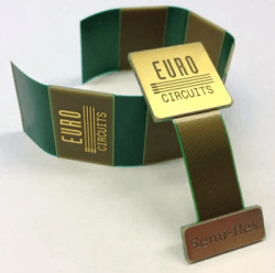
SEMI-FLEX pool
When a polyimide PCB is too expensive, the SEMI-FLEX solution is perhaps an option. This semi-flexible circuit board can be bent about 5 times. Beyond that there is a risk of damage. This is ideal for products where various circuit boards are mounted on angles to each other and so there is no need for continued flexibility of the connection. The semi-flexible circuit board is manufactured with four available copper layers, where the flexible part consists only of a 'core’ – a thin FR-4 core with a copper layer on both sides. The flexible connection between the boards is therefore not four-layer, but two-layer.RF pool
 Specifically for RF applications there is the RF pool service (RF meaning Radio Frequency). In addition to the full-service, mass production of RF circuit boards, you can also have small numbers of professional circuit boards made that are suitable for high-frequency applications through RF pooling. The main difference compared to PCB proto, is the base material that is used for this circuit board. Instead of FR-4, I-Tera® MT RF is used from Isola Group, or RO4350 or RO4003 from Rogers Corporation, but for the latter case the pool service is not available. These materials distinguish themselves from FR-4 through the (much) lower dissipation factor (Df) and the lower dielectric constant (DK). This reduces the effect that the printed circuit board material has on signals in the GHz range. For signals above 500 MHz these characteristics are essential if your circuit is to function as intended.
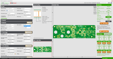
Stencil
For applying the correct amount of solder paste to the circuit board (for SMD) you use a stencil. Through this service you can have your own stainless steel stencils made, according to your specifications.IMS pool
 IMS stands for Insulated Metal Substrate. Instead of the familiar FR-4, 1.5 mm think aluminium is used as the base material. On top of this is an electrically insulated layer that is 100 µm thick, onto which the copper traces are attached. Subsequently follow the solder mask and silk screen (text layer). You use this technology, for example, when a copper surface is not sufficient to carry away the heat that is generated by (SMD) components. Because of this construction, this technology does not permit PCBs with more than one copper layer to be made. A plated-though via, for example, would lead directly to a connection to the aluminium base material and result in a short circuit between all vias.
Additional online tools
Even before you order a circuit board, you can use the online tools PCB Visualizer via the PCB Configurator and the PCB Checker to see whether the PCB can be manufactured as required and whether there are any sticking points. This can save a lot of time, money and trouble. In our opinion this is a bull's eye for Eurocircuits and the Visualizer tool brings the PCB production service to an outstanding and very comfortable standard!The Right PCB Design Solution
The Elektor PCB Service therefore offers for many common situations the most appropriate solution. From a few prototypes to medium-size production runs and from the most simple (NAKED) to the most demanding RF/SEMI-FLEX or IMS circuit board, it is all made very easily and intuitively, also thanks to the extensive online tools. For our prototypes we often use the service. You too?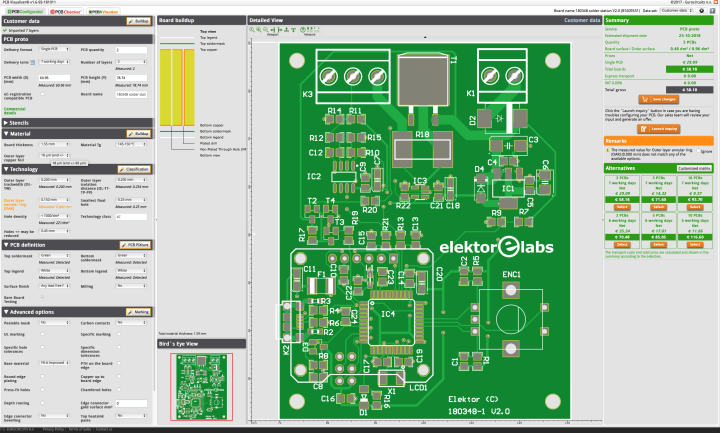
PCB Visualizer introduction:
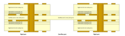
Production process of a four-layer PCB:
Read full article
Hide full article