
Review: Eurocircuits’ PCB Checker
Views
On each tab the issue categories are printed in bold green, the layers follow below. To see where a problem is, click on the layer of interest. The problem area will be shown in the Detailed View (where you can zoom even more) whereas the Bird’s Eye View shows which part of the board you are looking at in the Detailed View. Note that if there is more than one problem per layer they are all shown in the Bird’s Eye View; the zoom will show just one unless the other problems are nearby. The Fault View gives detailed information about the problem and also tells you how many there are. You can scroll through the issues with the back and forward arrows. The issue you are inspecting is shown in orange in the Detailed View (not in the Bird’s Eye View).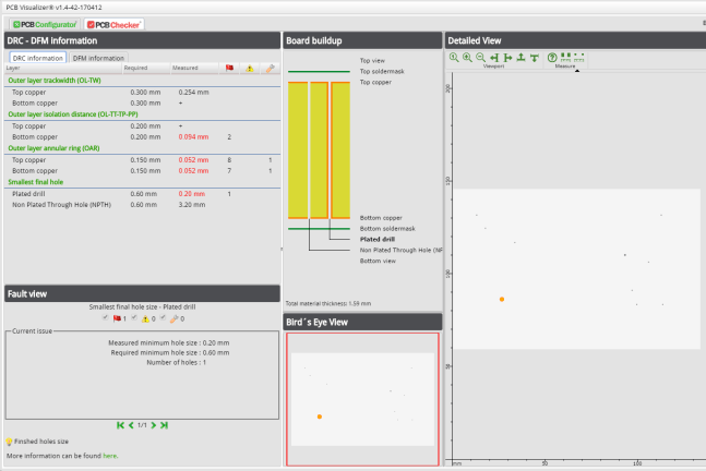
Issues
Critical issues are indicated with a red flag, non-critical issues by a yellow triangle with an exclamation mark inside. A tiny pliers icon is used for issues that can be repaired automatically. Critical issues usually indicate errors that should be fixed. Non-critical issues will very probably get fixed during manufacturing of the board, but it is, of course, best to fix everything yourself.For my board, the outer layer isolation distance (OL-TT-TP-PP) category lists issues on the bottom copper layer. The Bird’s Eye View shows two problems: a trace too close to a plane and a problem with a via. Huh? Looking closely at my design, I now discover that a trace that I thought was connected to a via in reality is not connected at all. Oops... Thank you, PCB Checker!
Clicking the layer under the outer layer annular ring (OAR) header reveals that all my vias are posing problems. Luckily I can solve this in my CAD program by changing the design rules for the vias. One of the vias is shown in green, meaning that it can automatically be repaired by the PCB Checker. However, comparing the repaired hole size (0.8 mm) to the size specified (1 mm) shows that maybe this is not a good idea, and it is probably better that I correct my design instead.
Read full article
Hide full article
Discussion (0 comments)