
How Eurocircuits handles your PCB design data and why
Single image preparation
In this stage an image of your order will be created that can be manufactured. The single image refers to the order; even if your design concerns a panel, it is still called a single image.It starts by saving a security copy of the PCB design data, and the netlist is extracted for later reference.
Now the hole sizes are adapted to the plating and drilling process. Plated holes (PTH) must be drilled a bit larger to accommodate the plating material. Non-plated holes (NPTH) are drilled slightly larger too because the PCB material “bounces back”, resulting in holes a bit smaller than intended.
Clean up & repair the copper
The copper must be cleaned up in many cases. This means that so-called “painted” features —solid elements that were filled by drawing line segments — are replaced by real polygons; minor imperfections which may cause problems in production are removed too.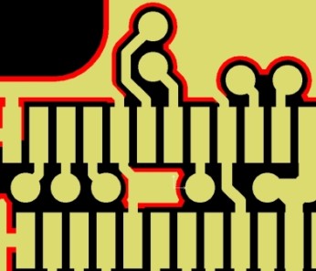
(Source: Eurocircuits)
The problems identified before as being repairable without user intervention are now repaired by adjusting the board’s copper. Tracks may be slightly moved, copper fills may be shrunken a little, thermals may be rotated, via drill sizes may be reduced, copper rings may be enlarged, but only as long as it does not result in an unrepairable isolation violation.
Solder mask & silkscreen
Once the copper layers are fine, it is time to clean up the solder mask. Missing openings will be highlighted as they may be unintended.Next in line is the silkscreen. Any print on bare copper will be removed; it will also be clipped back 0.1 mm from the solder mask. Order code, and optional UL marker and/or barcode are now added too.
Even more layers to prepare
After all these steps, the data is not yet ready. Still missing are the:- Drill drawing
- Route layer
- V-cut layer
- Solder paste layer
- Special layers (peel-off, via-fill, carbon)
- Customer panel
When these layers have been created, we arrive at the end of stage 2. A netlist is generated from the final data and compared to the one extracted at the beginning of this stage, and the new copper layers are compared to the initial copper layers. Any problems found will be corrected.
To top things off, a second engineer checks the final PCB design data against the customer’s order and against the specifications of the chosen service.
Read full article
Hide full article
Discussion (0 comments)