DDR5 is a game changer in DDR memory technology. DDR5 is designed to satisfy large performance demands for data centers. Several key drivers for this technology are smart mobile technology and exascale computing. CPUs in the server and high computing industries are each fueled by GBs of memory. Technologies such as IoT, 100/400GBE and 5G are now connecting the world in real time. Storage architecture has been redefined with nonvolatile memory moving closer to the CPU. Also, the rise of new technology spaces like artificial intelligence and machine learning are defining the role of memory today.
by Ailee Grumbine, Strategic Product Planner, Keysight Technologies, Inc., Data Center Industry Solution Team
DDR5 uses an explicit full rate clock. The clock signal clocks the command signal and the strobe signal clocks the data. The bus is wide and single ended. A server blade may contain over a thousand parallel data lanes. The read and write commands are bidirectional. This means that read and write data overlaps. Unlike other serial bus signals, the strobe and data can be bursty with idle states. DDR5 will operate at a much higher speed in comparison to its predecessor. It is known that DDR5 will be at least double the speed of DDR4. This means there are several characteristics of the signal that need to be tested and verified differently than DDR4. DDR1, DDR2, and DDR3 operate up to 2133 MT/s.
Hyper speed
The signals use high speed transmission lines where timing and impedance are problematic for designers. DDR4 technology is where the big change happened. DDR4 operates up to 4200 MT/s and is considered a high-speed serial bus. Validating the data valid window with eye diagrams and receiver masks is a key task for the designer. Now with DDR5 operating at the hyper speed of 6400 MT/s, the big question is: can an open eye be achieved? If so, the tests used for the design stage of DDR4 will also apply to the design stage of DDR5. If not, we may need to use techniques like equalization to open the DDR5 eyes, as is often done with serial buses.
Signal integrity is a big issue in characterizing DDR5 DRAM transmitters. The number one challenge when it comes to testing a DDR5 design is the ability to separate read and write data. Legacy methods, such as using strobe and data signals or identifying the read and write pre-amble pattern, may no longer be applicable. Since signal integrity is going to be a major challenge, new test parameters may be required in addition to legacy timing and electrical and eye diagram tests. Jitter may also now become an important component for characterization in the design. Faster data rates especially at speeds higher than 3600 MT/s may cause the eye to close.
This means that every little bit of margin counts. Great consideration should be placed on noise and jitter performance when choosing any test equipment. New methods to characterize the data will also be required if there is no eye. It may be that an equalization method, such as decision feedback equalization, is needed to open the eye for making any eye diagram measurement.
Access to the signals
Before we can do any characterization work, however, we first need to gain access to the signals of interest such as clock, strobe, data, and command. If there are vias available, they are the best place to access these signals because you can probe directly at the balls of the DRAM. However, via access is limited, especially when boards are loaded with multiple devices with as little keep out volume as possible.
The next option would be to use a BGA interposer. The interposer routes out all signal of interests for testing. It is soldered using a BGA rework station to the board and the DRAM is soldered onto the interposer with a BGA rework station. ZIF or micro probe heads are used to provide the connections to the oscilloscope. It is very important to not break the bus when you load the interposer.
Data eye testing
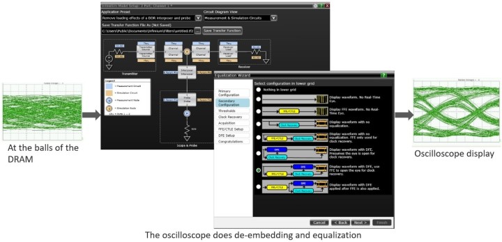
The designer must make sure the interposer is designed to handle the speed of the signal with very minimum loading. Even if the interposer doesn’t break the bus, you would probably need to de-embed the signals. Use the S parameters files in the de-embedding software to build a transfer function file, which would correct the frequency response of the signal. At higher data rates, above 3000 MT/s, eye collapse at the ball of the DRAM is anticipated due to inter-symbol interference. DDR5 will probably require equalization, such as decision feedback equalization, to improve the data eye after being latched by the receiver. The equalization method used needs to be able to open the up the eye without amplifying the noise due to reflection (Figure 1).
Figure 1: Equalization method being used to open the closed eye at the balls of the DRAM.
Margin is going to be much tighter in DDR5. This means that we need to do characterization of timing and signal integrity to make sure timing is met between the key signals, such as clock, strobe, data, and voltage requirements. In LPDDR4, JEDEC introduced the tDQS2DQ test, which measures write cycles timing to the DRAM. The test tells the DRAM designer how much skew is allowed by the controller so that the controller doesn’t have to deal with huge variations in the DRAM.
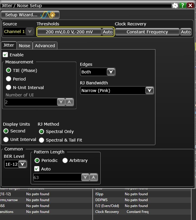
It is one of the more critical DRAM compliance tests, which will be critical for DDR5 as well. For jitter characterization, it is important to be able to separate random and deterministic jitter components (Figure 2). This allows the designer to identify the source of any potential noise, crosstalk, or duty cycle distortion. A data eye test is a standard method used to verify the data valid window.
Figure 2: N-unit interval jitter measurement setup on an oscilloscope to measure
random and deterministic jitter.
A data eye test makes eye height and eye width measurements. If the eye is closed, an equalization method will need to be used to open the eye. Eye width and eye height measurements need to account for noise of the instrument. This is true for jitter measurements as well.
DDR5 design complexity warrants design cycles that include simulation, analysis, and debug and compliance testing. The design workflow will need to allow data analytics capability to perform measurement correlation between simulation, design of experiments, and compliance. Modern simulation tools allow output of waveform files to be used in the compliance test software for early testing before a real device under test is available.
If any of the tests fail, early redesign or optimization work can be done with the help of a data analytics tool to find the optimization point. Then when an actual device under test is available, measurement correlation can be performed to further refine the performance and margin of the design.
Conclusion
In summary, the key to successful DDR5 transmitter testing depends on what tools you use to perform the measurements. A complete DDR5 transmitter solution consists of a probe, an oscilloscope, and a compliance or validation software which will cover all the test speed and test parameters.
When choosing an oscilloscope, make sure it has the lowest jitter and noise performance. You want to use an automated software package for compliance or validation work to ensure interoperability and repeatability. You can perform the measurements manually with an oscilloscope but translating the test parameters into measurement steps can be tedious and will take up more test time.
The Author
Ailee Grumbine specializes in data analytics and high-speed memory technologies such as DDR and SD UHS interfaces. She graduated from the University of Science Malaysia in 2001 and completed a Masters of Business Administration from the University of Colorado, Colorado Springs. Prior to her current position, Ailee was a regional applications engineer with expertise in high-speed bus applications which include DDR memory physical layer and protocol testing. (190239)


 The Author
Discussion (1 comment)