
Relay Logic Goes Nano
on
In an effort to bring the advantages of relay logic to the modern world of miniaturized devices, research groups in various parts of the world are exploring ways to develop nanoscale mechanical relays that can be used to build process controllers. Although typically slower than semiconductor logic devices, relays have the advantage of very low quiescent power and bidirectional current flow. Nanoscale relays can additionally achieve significantly higher switching rates than their normal-scale cousins.
To support this effort, the European Commission has put IBM Research Zurich, in collaboration with STMicroelectronics, in charge of a European research project that aims to develop a logic process based on nanoscale relays that are compatible with conventional CMOS transistor logic. Academic researchers at the École Polytechnique Fédérale de Lausanne (Switzerland), Kungliga Tekniska Högskolan (Sweden), and the Universities of Bristol and Lancaster (UK) are also involved in the project. The rationale for the research is that leakage power consumption is becoming as large as active power consumption with increasing semiconductor device miniaturization, which is especially significant for applications such as autonomous sensor nodes, wireless communication and mobile computing.
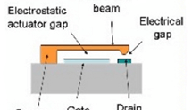
The Nano-Electromechanical Integration and Computation (NEMIAC) project aims to develop a process based on nano-electromechanical switches (NEMs) that is suitable for embedded systems and enables 3D integration with CMOS. The researchers are asked to demonstrate an order of magnitude improvement in energy efficiency with no performance penalty compared with semiconductor devices. The process is also expected to have higher radiation resistance and tolerate higher operating temperatures than CMOS. The relays are expected to have a footprint of less than 3x3 microns and a switching time on the order of 10 ns. Demonstrating reliability for billions of switching operations will be an important task prior to commercial deployment.
Discussion (0 comments)