
Programming PICs from the Ground Up
on
For software development, we will use the Microchip Technology MPLAB X Integrated Development Environment (IDE) and a PIC 16F18877 as our target device. Programming takes place using the ICSP interface, so you have freedom to choose any development board for this device (a prototyping plug-board will also do).
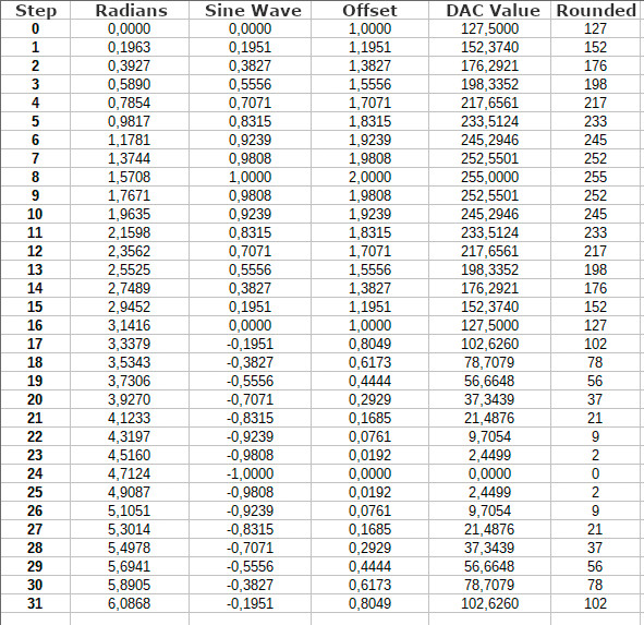
To produce a continuous ‘digitized’ sine wave from a DAC, we have to supply it at regular intervals with digital values corresponding to voltage levels of a sine wave. Here we use 32 discrete values for every period. Microsoft Excel can be used to generate the sin() function values. The Excel table shown in Figure 1 shows the time intervals from 0 to 31 in the column on the left. The formula =A2*((2*PI())/32) provides us the values. The values are for a period from 0 to 2π radians. The third column contains the sine values of the radians in column 2 =SIN(B2). These values are in the range of -1 to +1, but the DAC can only work with positive values. To resolve this, we add a fixed offset to all the values =1+C2 so that the range of -1 to +1 now is in the range 0 to 2 i.e. all positive. The adjusted values are scaled using D3*(255/2) so that they are in the range 0 to 255 which corresponds with the 8-bit input values expected by the DAC. Finally, the values are rounded using ABRUNDEN(E10).
Tables in Data Storage
The values corresponding to a sine wave function are constants so they can be stored in a table in memory. To retrieve a value in the table we can use the RETLW instruction that returns with the table value in W (the accumulator).
In assembler we can define an area in memory where the table will be located. In higher-level languages, we are normally not bothered by such details and the compiler will work all this out for itself. We could start the area almost anywhere but, as we will see later, there are some benefits if we start the table at certain addresses. Here we define the start address of the table at 0x200:
TABLE_VECT CODE 0x0200
dt 127, 152, 176, 198, 217, 233, 245, 252, 255, 252, 245, 233, 217, 198, 176, 152, 127, 102, 78, 56, 37, 21, 9, 2, 0, 2, 9, 21, 37, 56, 78, 102
END
The dt (define table) directive stores the values provided as a table in memory. This small code fragment can be put through the assembler. The MPLAB assembler ignores many critical situations so when it does throw up a warning such as:
Warning[202] C:\USERS\TAMHA\MPLABXPROJECTS\CH6-DEMO1.X\NEWPIC_8B_SIMPLE.ASM 72 : Argument out of range. Least significant bits used.
it’s important to take it seriously and find out what the problem is; mistakes are an essential part of the learning process. How we have defined the table is incorrect, but this makes for a good opportunity to undertake some experimentation.
Assembling and Disassembling
Except when macros are used, there is a direct connection between mnemonics and machine code. Machine code is created by assembling the mnemonics, while the reverse process is performed by a disassembler.
Double-click the Usage Symbols disabled (Figure 2) tab at the bottom right of the display. Select the Load Symbols when programming or building for production checkbox so that the analysis tools are used in the compilation process.

After clicking on Apply, run the compiler again so that the memory usage can be displayed. The option Window > Debugging > Output > Disassembly Listing File Project tells the compiler to display a disassembled version of the original code section. This can be useful because it shows us how the compiler has handled the code (Figure 3).

The output consists of six columns, with the numbers on the far left describing the ‘logical’ address of the word in the program memory of the PIC. The next column is the decimal equivalent of the command. The third column contains the disassembled version generated from the hex machine code (for example, constant or variable names and comments in the original assembler file cannot be included). The fourth column specifies the line number in the .asm file and, after the colon, there is the respective line that is responsible for the binary word to the left.
Now we can see that the assembler has by default assumed the values we stored in the table are hexadecimal as it has only used the last two digits of each number (in the 8-bit world, a hex value consists of two characters):
0200 3427 RETLW 0x27 73: dt 127, 152, 176, 198, 217, 233, 245, 252, 255, 252, . . .
0201 3452 RETLW 0x52
0202 3476 RETLW 0x76
0203 3498 RETLW 0x98
0204 3417 RETLW 0x17
0205 3433 RETLW 0x33
. . .
Values entered into such tables can be any of hexadecimal, binary, octal, decimal etc., so it’s necessary to use a ‘base indicator’ symbol before each value. This will let the assembler know that, in this case, the values are decimal. This is done by preceding each value with a decimal point (i.e. a period or full stop). Now, during assembling, the compiler will take the maximum (8-bit) decimal value of 255 and convert it into the maximum hex value FF for use in the code. The table now looks like this:
TABLE_VECT CODE 0x0200 dt .127, .152, .176, .198, .217, .233, .245, .252, .255, .252, .245, .233, .217, .198, .176, .152, .127, .102, .78, .56, .37, .21, .9, .2, .0, .2, .9, .21, .37, .56, .78, .102
END
Accessing Tables
To retrieve information stored in the table, we use the RETLW instruction to jump to the table. On returning, the W register (the accumulator) will contain the value from the table. To understand the process we will first convert the start address of the table 0x0200 into its binary equivalent which is 0000 0000 0000 0010 0000 0000 0000 0000.
Calls to locations in the program memory can be made using the CALLW instruction, and Figure 4 gives more detail on how this instruction works.

The full program memory address space of the PIC contains 32,768 words, which requires a 15-bit address pointer to access the full memory space. Instructions like CALLW use the W register to pass the program pointer value (pointing to the location in memory where the subroutine begins). W is only 8-bits long, so it’s necessary to make use of the PCLATH register to store the upper value of the program counter proior to the call.
To reduce unnecessary work and possible timing conflicts, the PIC will only use the value of PCLATH if it is required. We can assemble the pointer values in the registers before making the call. Writes to PCLATH leave the current value of the program pointer unaffected. Initialization of the program begins by incrementing the run value:
WORK
BANKSEL DAC1CON1
MOVLW B’00000001’
ADDWF PortCache, 1
By checking the full binary address given above we can see what value needs to be loaded to the upper part of the program counter. This value is transferred to PCLATH via the W register using:
MOVLW B’00000010’
MOVWF PCLATH
Now we are all set to make the jump. Executing CALLW results in the value from the table being returned in the W register. This value is then passed to the DAC to output the corresponding analogue voltage level:
MOVFW PortCache
CALLW
MOVWF DAC1CON1
CALL WAIT
Now, if we try executing the program the controller runs until MPLAB stops execution at some point.
The reason is that the table consists of 32 values but the program is working with 255 values. The additional memory locations may contain random values from previously installed firmware. As the pointer increments the program finds itself running into unchartered territory.
This next code section limits the range by subtracting 31, detecting if the zero flag is set by the operation, and then using CLRF with PortCache:
MOVFW PortCache
SUBLW .31
BTFSC STATUS, Z
CLRF PortCache
Finally, we need to jump back to the start of the loop:
GOTO WORK ; loop forever
Now we can run the program. The output shown in Figure 5 looks pretty chaotic and nothing like the sine wave we were expecting. The reason for this is that the DAC in the processor only accepts values in the range from 0 to 31 but we are supplying values in the range 0 to 255.

Tables from Memory
We could resort to Excel to produce the scaled-down values we require for the sine wave and use them in the table, or we could use the processor to carry out the necessary division of the values in software.
However, using assembler we have direct access to binary values stored in registers. The simplest method to carry out a divide-by-2 operation on a binary value is to shift its pattern of ones and zeroes in the register one place to the right. This ignores any carry bits and shifts a zero into the most significant position in the register. To convert values in the range 0 to 255 into the range 0 to 31 we need to divide the value by eight. This corresponds to shifting the value in the register to the right three times.
When the values are copied into memory, we have to calculate target addresses. To do this, we look at the Core Registers. PCLATH is already known, but we are also interested in INDF and FSR. Our PIC has two 16-bit File Select Registers (FSR). These are able to access all file registers and program memory allowing one Data Pointer for all memory. The Indirect File Registers (INDF) are not physical registers. An instruction that accesses an INDFn register accesses the register at the address specified by the File Select Register (FSR). Write operations to the program memory cannot be made via the INDF registers.
A special feature of the PIC is that the choice between program and working memory is made via bit 7 of the FSRxH register. If it is set, the label points to a location in program memory; if not, it addresses data memory.
We start again by storing the variables. This time we need a total of 32 bytes of memory - an allocation size too big to be used as a ‘shared’ memory facility.
We access memory in a bank to be selected by assembler and work with relative addressing. Additional parameters have not been specified so MPASM grants free choice in the position of the DataBuffer:
udata_shr
LoopC res 1
PortCache res 1
udata
DataBuffer res 32
The high and low parts of the address remain uncertain. Fortunately, the linker makes our work easy with two Operators:
START
MOVLW high DataBuffer
MOVLW low DataBuffer
With this knowledge, we can copy information from the program memory into the main memory. Shift operations do not work directly in W so an additional variable is required:
udata_shr
LoopC res 1
PortCache res 1
WorkArea res 1
The initial condition is important when working with data tables. We preload PortCache with 1111.1111 because the loop increments before it is used. The first pass therefore increments it to 0. If we had preloaded with 0, the first pass would skip 0 and write to location 1:
START
. . .
MOVLW B’11111111’
MOVWF PortCache
MOVLW B’11111111’
MOVWF LoopC
The program consists of two loops: the PREP-loop prepares and writes the table of sine wave values to a table, while the Work loop sends the values to the DAC so that the signal waveform can be output. PREP begins with an access to the table:
PREP
MOVLW B’00000001’
ADDWF PortCache, 1
MOVLW B’00000010’
MOVWF PCLATH
MOVFW PortCache
CALLW
Now, with the value in W, we need to move it to the F register and perform three rotate right instructions to divide its value by 8:
MOVWF WorkArea
BCF STATUS, Z
RRF WorkArea, 1
BCF STATUS, Z
RRF WorkArea, 1
BCF STATUS, Z
RRF WorkArea, 1
To avoid errors generated by the state of the carry bit in the status register, BCF STATUS, Z is used to clear the carry flag in the register before each shift operation. The listing contains two small errors which will prove interesting to resolve.
Now we need to ensure that INDF points to the correct memory location: To achieve this, the registers FSR0H and FSR0L are loaded with address data. The H register (high) contains the higher part and the L register (low) the lower part:
MOVLW high DataBuffer
MOVWF FSR0H
MOVLW low DataBuffer
MOVWF FSR0L
INDF0 now points to the beginning of the memory area. We need to add the offset that identifies each location. It is not certain that the beginning of the field is at the beginning of a page. If there was an overflow when adding the offset in the L part, the H part would not notice this. As a solution to this problem, the status of the C bit is checked and the value of FSR0H is incremented if there is an overflow:
MOVFW PortCache
CLRC
ADDWF FSR0L
BTFSC STATUS, C
INCF FSR0H
The CLRC (Clear Carry) command is a macro that clears the C bit in the status register. This ensures INDF0 is correctly configured. We have to load and write out the value temporarily stored in the work area:
MOVFW WorkArea
MOVLW INDF0
Finally, we need to make sure that the loop keeps running:
MOVFW PortCache
SUBLW .31
BTFSS STATUS, Z
GOTO PREP
CLRF PortCache
As the code is starting to get more involved and complex, it would be helpful to use some of the IDE tools to examine program execution more closely and verify correct operation.
Troubleshooting in Assembler
Placing breakpoints is theoretically easy; click on the line numbers in the IDE to place a red stop symbol. However, since the microcontroller can only manage one hardware breakpoint, this causes a message to appears. MPLAB uses up debugging resources to enable it to run in stages. We do not require breakpoint emulation at the moment, so we can remove the message by clicking No. As the PIC supports software breakpoints, you can affirm with Yes.
As long as you place more than one breakpoint in the assembler file, Microchip activates this function automatically.
Our PIC will only support one hardware breakpoint. Click on the down arrow next to the debugger symbol in the toolbar and select the Debug main project option. MPLAB opens a disassembly window that we can then close. After reaching the breakpoint, the IDE shows the status as in Figure 6.

The line with the green background and right-pointing arrow in the line number column on the left is the current instruction. Symbols in the toolbar, such as stop and jump, allow user interaction with program. Window Target Memory Views File Registers opens a window to view the PIC memory space. Place a cursor like the mouse pointer over the DataBuffer Declaration. This opens a tooltip window with the address of the first byte and its value. On the author’s workstation this position is 0xD20.
It is more convenient to click the blue arrow (GoTo) in the File Registers window. In the GoTo What box, select Symbol and select DataBuffer. Close the popup after clicking the GoTo button to see the result shown in Figure 7. The red highlighted box is the first byte of the table. It is obvious there is an error because other values shown in the table such as FC are outside the permitted range.

To investigate we can fill the memory area with an easily recognizable bit pattern. A good example would be to write the value 11111111 into the indirect register:
MOVFW PortCache
CLRZ
ADDWF FSR0L
BTFSC STATUS, C
INCF FSR0H
MOVFW B’11111111’
MOVLW INDF0
If you view the code in the debugger, you will see a sequence of the same values. In most cases, they should not have the value FF. The code has a small error. We can use the MOVLW instruction to load the value of a memory location into the W register:
MOVFW B’11111111’
MOVLW INDF0
From MPLAB's point of view, the literal INDF0 is a number: after compilation, values like PORTA are just numbers. So our program copies the address of the register into all 32 memory locations. Nevertheless, we are one step further since we have already verified the address data. A corrected version of the program now looks like this:
MOVLW B’11111111’
MOVWF INDF0
Now that the memory address calculation works, we can eradicate the actual calculation error. The first problem was using the MOVLW instead of the MOVWF instruction, which made writing to INDF impossible:
MOVFW WorkArea
MOVWF INDF0
MOVFW PortCache
SUBLW .31
BTFSS STATUS, Z
GOTO PREP
When looking at the output, we can see that the values are not correct. The cause of this problem is that the RRF instruction can set the carry bit. Our code however has only taken care of the Z flag; we need to make a small correction:
MOVWF WorkArea
BCF STATUS, C
RRF WorkArea, 1
BCF STATUS, C
RRF WorkArea, 1
BCF STATUS, C
RRF WorkArea, 1
The program is now ready to run and the table of sine wave values appear in the debugger window. For completion, we have to ensure in the working loop that the values are taken from the data memory. This requires an increment of the run variable in order to generate a continuous index:
WORK
BANKSEL DAC1CON1
MOVLW B’00000001’
ADDWF PortCache, 1
Indirect addressing is suitable for reading and writing. We load the two parts of the address of the buffer in FSR0H and FSR0L. Then we add the offset and check for an overflow. If an overflow occurs, we increment the upper register:
MOVLW high DataBuffer
MOVWF FSR0H
MOVLW low DataBuffer
MOVWF FSR0L
MOVFW PortCache
CLRZ
ADDWF FSR0L
BTFSC STATUS, C
INCF FSR0H
What is new is that we are reading from register INDF0. The value is loaded into the DAC1CON1 register of the DAC:
MOVFW INDF0
MOVWF DAC1CON1
CALL WAIT
The rest of the program is an ordinary loop that, among other things, takes care of the increment operation:
MOVFW PortCache
SUBLW .31
BTFSC STATUS, Z
CLRF PortCache
GOTO WORK
With that the program is finished and you can see the resultant sine wave output signal in Figure 8.

Conclusion
This project shows that interesting experiments can still be implemented with 8-bit microcontrollers. More information on this topic can be found in my new book Microcontroller Basics with PIC. If you enjoyed this article, please let me know. I always welcome constructive feedback!
(200154-02)
----------------------------------------------------------------------------------------------------------------------
Want more great Elektor content like this?
--> Take out an Elektor membership today and never miss an article, project, or tutorial.
----------------------------------------------------------------------------------------------------------------------
Discussion (1 comment)