
Breakout Board: Increase the Number of I/Os of Your Development Board
on
Are you tired of trade-offs due to the lack of I/O ports while developing your designs with the preferred platform? Do you want more to handle your multitude of signals and actuators? This breakout board, managed via I²C bus, will allow you to add up to 16 I/Os per unit, until a maximum of 128 I/Os on your existing system.
There are various practical situations in which it is necessary to manage several signals and actuators with a microcontroller, which, however, does not have enough I/O pins; in such situations, it becomes useful to resort to those integrated circuits known as I/O expanders, whose function is to serialize a certain number of input and output lines to control them via a single I/O, i.e., a serial communication line such as the common and very widespread I²C Bus, found in many microcontrollers and, not least, in Arduino boards.
To meet the need to multiply (expand, in fact, as the same term "expander" suggests) the I/O lines, we have made the breakout board based on the MCP23017, which we propose in this article, on which we find such a Microchip integrated circuit that is, as can be expected, a 16 bit I/O expander, as well as the minimal hardware to make it work, which in this case consists of a dip-switch and some pull-up resistors. Finally, to give you an idea of what can be accomplished with an I/O expander, we will propose an application example where the breakout board drives a series of relays (eight in all) mounted on a board that can be driven via TTL levels or button presses. But let's go in order and analyze the circuit diagram first.
Breakout Board Circuit Diagram
As you can see in the schematic diagram in Figure 1, the breakout board is something extremely basic, since on board there is the MCP23017 integrated circuit in DIP (traditional mounting) version, with all the pins - which on the PCB are 2.54 mm pitch — to ease the future mounting of pin-strips, for insertion in other boards or breadboards — except for the three for setting the least significant bits of the peripheral I²C Bus address. To this purpose, a 3-way dip-switch (labeled SW1 in the wiring diagram) was provided, to set the communication address on the I²C Bus, whose pins A0, A1, and A2 are pulled-up by resistors R1 to R3 that keep them at logic level High when the switches are open.
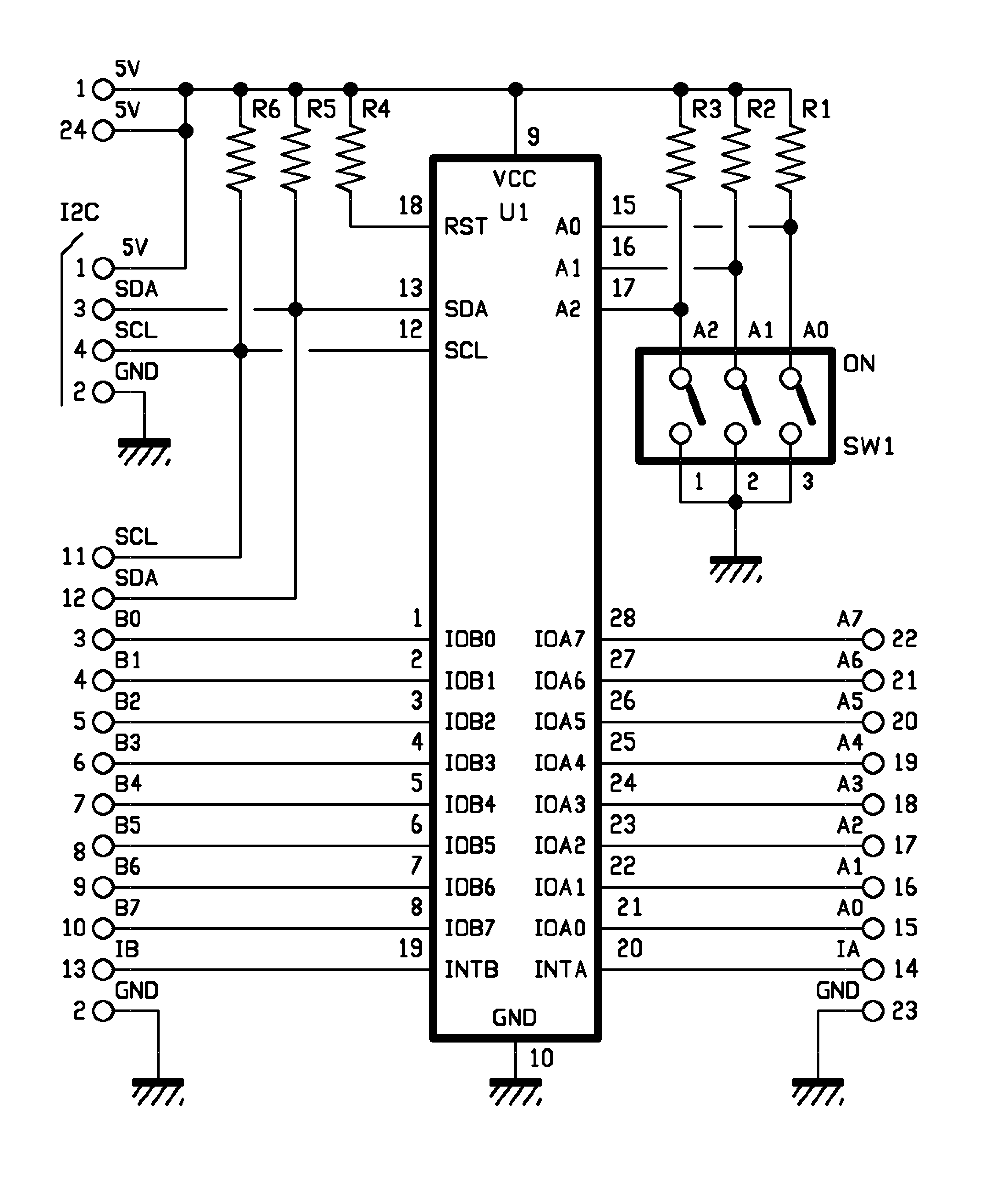
Figure 1: The schematic diagram of the breakout board.
To summarize, all I/O-related pins of registers A and B were ported outward on male pin strips. These pins have been arranged on both sides so that we can connect our board with ease, but of course they are digital I/O pins; therefore, you can connect anything you want, within the limits of the current and voltage supported by the MCP23017 IC. In addition to the 2.54 mm-pitch side pin strips, which also allow the module to be housed in a breadboard, another 4 pins have been provided on a strip (also 2.54 mm-pitch) called I2C so that we can connect to the bus directly at the top of the module. It is understood that the side pins alone are sufficient for communication and interfacing with the module; therefore, the four pins of the I2C connector are placed in parallel with those already existing on the board.
Note that on the circuit board, for convenience, the A register pins have been placed on one side and the B pins are on the opposite side, again with the purpose of simplifying connections. The pins belonging to the I²C bus have been returned to the pin-strip marked I2C, along with the 5 V positive and ground; both have pull-ups. The I/O-expander reset in our breakout board is not used; therefore, to disable it, we placed the relevant pin (18, RST) at logic level High via resistor R4.
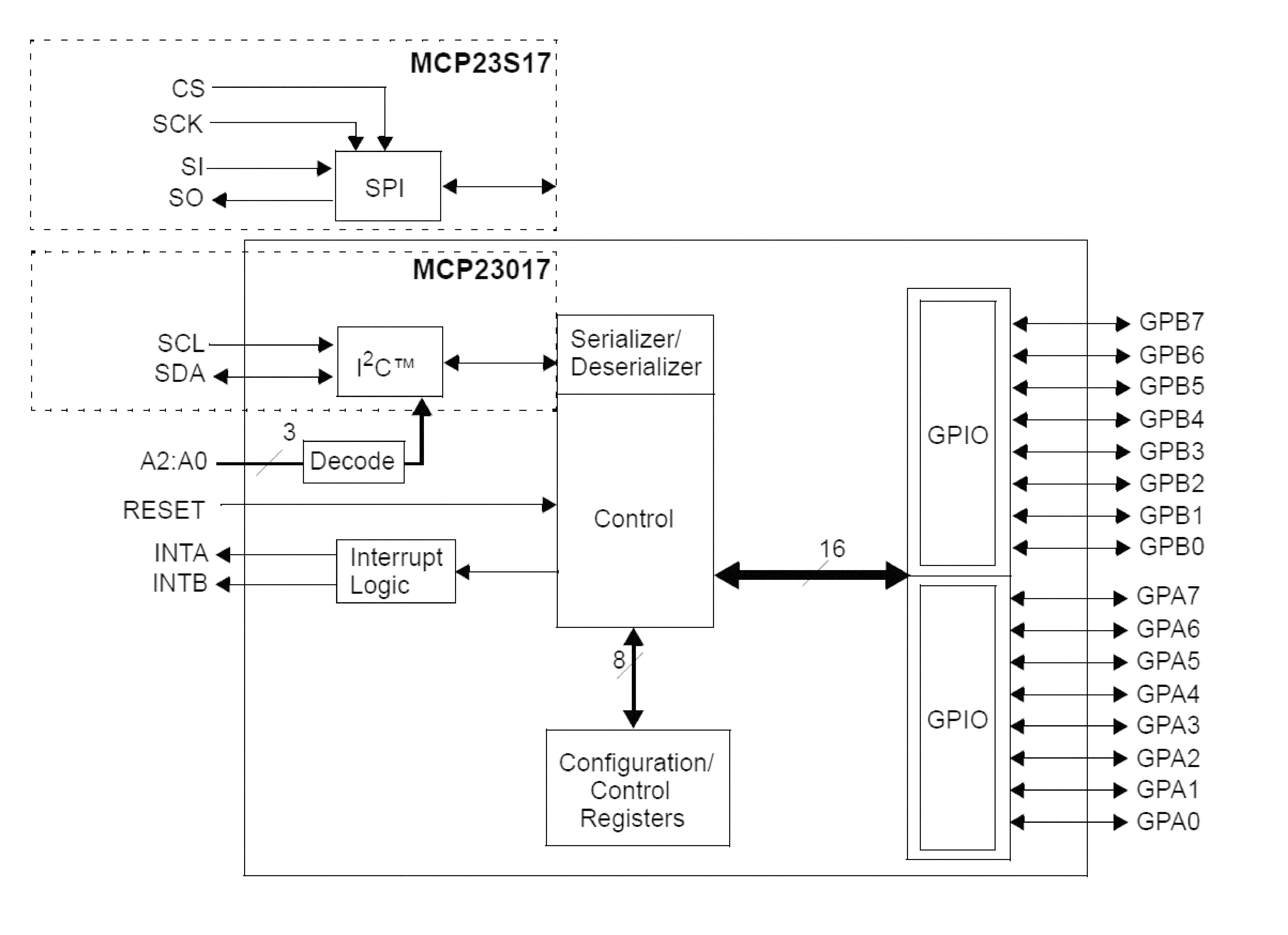
Between the side pins of the board we also find repeated GND and +5 V lines. The main element of the circuit is, of course, the MCP23017, which we can consider to be an I²C Bus/parallel converter, manufactured by Microchip (marked U1); the integrated circuit, of which you see the internal block diagram in Figure 2, functions as a peripheral (Slave) of the I²C bus and supports the two input and output modes. In the former, it allows the I/O states of the A and B registers to be transferred to the bus in serial format, one byte for each register, at the request of the I²C Bus Master device; in the latter, it goes to set the I/O lines by converting the incoming data on the I²C bus to the corresponding state of the A and B register lines.
The MCP23017
The chip at the core of the breakout board described here is an I/O expander with 16 bits, divided into two ports of 8 bits each, interfaced via I²C-Bus; this means that with only two wires, referenced to ground, it allows you to acquire the status, or set it as the output, of as many as 16 lines.
Its technical characteristics are as follows:
- High-speed I²C data interface, operating at 100 kHz, 400 kHz or 1.7 MHz
- I²C-Bus address settable in 8 combinations
- Configurable interrupt pins, by level and logic function
- Configurable interrupt source
- Reversed polarity register
For the inputs:
- External reset input
- Standby current of 1 μA max.
- Supply voltage from 1.8 V to 5.5 V
The MCP23017 integrated chip provides 16-bit generic serial/parallel I/O expansion and is available in two versions: the one used here, equipped with an I²C Bus interface, is the MCP23S17, an SPI interface variant. The chip is a 16-bit I/O-expander, divided into two ports of 8 bits each, interfaced via I²C Bus; this means that with only two wires, referenced to ground, it allows the acquisition of the state of as many as 16 lines (input mode) or setting the logical state of each of them (output mode). The I/O lines are, by default, operating as inputs.
The MCP23017 consists of multiple registers in 8-bit configuration for input, output, and polarity selection. The system master can enable the I/Os as inputs or outputs by writing the corresponding I/O configuration bits (IODIRA/B). Data for each input or output is stored in the corresponding input or output register. Input Port register polarity can be reversed using the Polarity Inversion Register. All registers can be read from the system master. The 16-bit I/O port is structurally composed of two 8-bit ports, namely port A and port B, which are headed by pins, 21÷28 and 1÷8, respectively. The MCP23X17 can be configured to operate in either 8-bit or 16-bit modes; furthermore, it has the two interrupt pins, INTA and INTB, which can be associated with their respective ports (INTA for Port A and INTB for Port B9 or can be subjected to the logical OR operation so that both of these pins will activate if both ports result in an interrupt.
The interrupt output can be configured to trigger under two (mutually exclusive) conditions:
- when an input state differs from its corresponding input port register state; this condition is used to indicate to the system master that an input state has changed;
- when the state of an input is different from the preconfigured value of the register (DEFVAL register).
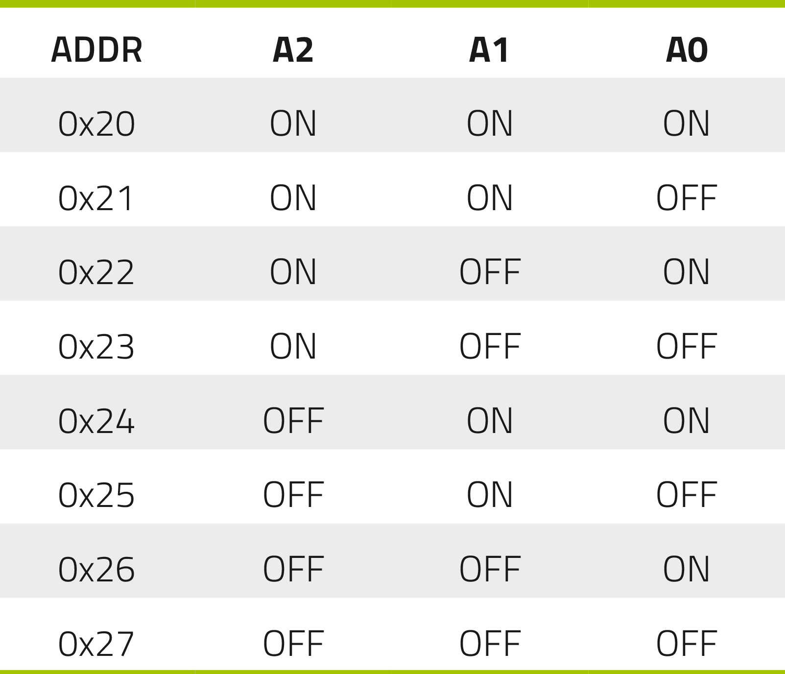
The INTA and INTB interrupt lines can be configured as active-high, active-low or open-drain. The Interrupt Capture register captures the values of the ports at the time the interrupt is triggered, thus storing the condition that caused the interrupt. The Power-On-Reset (POR) sets the registers to their default values and initializes the device state machine. The need for bidirectional operation is due to the fact that each I²C Bus peripheral must both be able to read (e.g., commands) and be able to send acquired, 8+8 bit data along the bus. Like all units for I²C Bus, the MCP23017 allows its address to be set in a range of 8 addresses, and for this purpose it has pins A0, A1, A2, which allow the addresses of the Slave unit to be set, if addressed directly from the I²C Bus; each of these lines is set through a dip-switch switch SW1: each closed dip sets the logical zero on the respective address, while, vice versa, an open dip determines the logical state 1. The ability to define eight addresses allows up to eight I/O-expanders to be placed on the same bus and thus control a maximum of 128 I/Os with only three lines.
The entire circuit is powered by the 5 V contact (we actually have two contacts: 1 and 15, located on the long sides of the breakout board) referenced to ground (GND contacts, i.e., 2 and 23 of the side rows). With this hardware, the logic of operation is as follows: whenever it receives a string along the SDA line of the I²C Bus (paced by the clock signal on the SCL line), the MCP23017 integrated circuit executes the command contained therein (in this case the one indicating to load the data byte) and arranges the 8 output lines IOA0÷IOA7 and IOB0÷IOB7 as the relevant bits, i.e., IOA0 will assume the state of the first bit of byte 1, IOA1 that of the second bit, and so on. The same will occur on IOB0÷IOB7, which will exactly replicate the bits of the second data byte.
Of course, conversion and presentation on the outputs occurs only assuming the received string contains the I²C Bus address corresponding to the one set, via the dip-switches of SW1, for U1. When each string is received, the integrator updates the status of its outputs, and the respective logic levels determine whether the LEDs of the display segments are turned on (or remain in the off state); if no string is subsequently sent, the display retains the displayed number because the outputs of the MCP23017 integrator are latch. The above applies to output mode, i.e., writing the status of the two I²C-Bus bytes to output registers A and B; if, on the other hand, the command coming from the bus is read, the MCP23017 acquires the I/O status of each register and generates two bytes, the first containing the status of IOA0÷IOA7 and the second the logical condition of IOB0÷IOB7; it then sends them along the I²C bus as a response. For each application to which you will want to allocate the breakout board, in Table 1, we give you the correspondence between the addresses and the dip-switch setting.
Practical Realization
Well, now that we have described the wiring diagram, we can move on to the construction notes; then we will propose an application example based on interfacing with an Arduino board accompanied by the corresponding sketch. As usual, we have drawn a printed circuit board available for download (it's a double-sided board); from them, you can proceed to prepare the PCB by photoengraving; after you'll have etched and drilled it, you can assemble the very few components needed, which, in this project, are all traditional, TH-type, for those who do not like the SMT technique too much. First insert and solder the resistors, then proceed with the socket for the integrated circuit (to be placed with the notch facing as shown in the assembly plan you see in this article) and the 3-way dip-switch, to be mounted with switch 1 facing left, looking at the board with the socket for U1 on top.
Finally, insert and tin into the respective holes the 4-pin strip marked I²C, and then, on the opposite side of the PCB, insert and tin two rows of 12 pins headers that will allow mounting on breadboards or insertion on other boards, i.e., to eventually connect with Arduino using classic male/female wire jumpers. Once you're done soldering the components, insert the MCP23017 into the socket, holding it with the notch facing as shown in the mounting plan on these pages. With that done, your breakout board is ready for experimentation or prototyping.
Let's Use It With Arduino
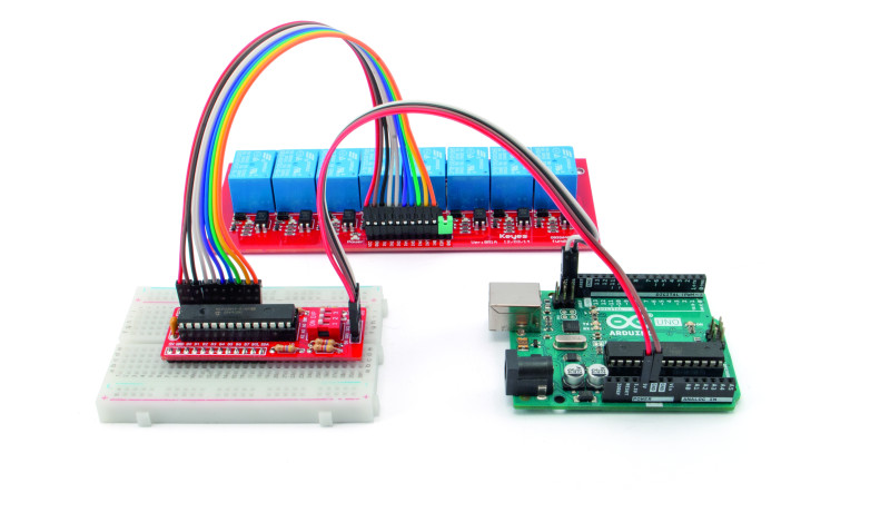
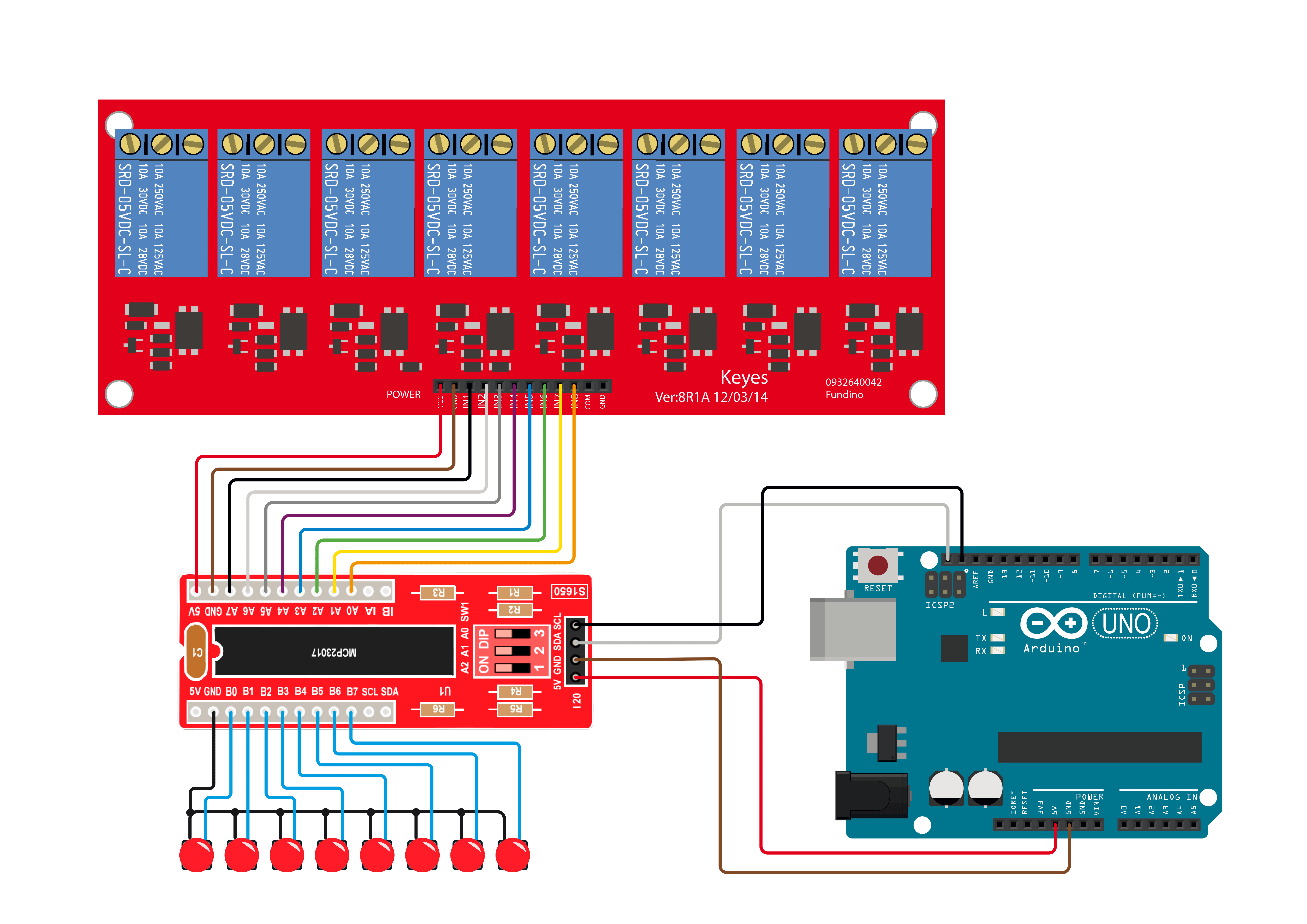
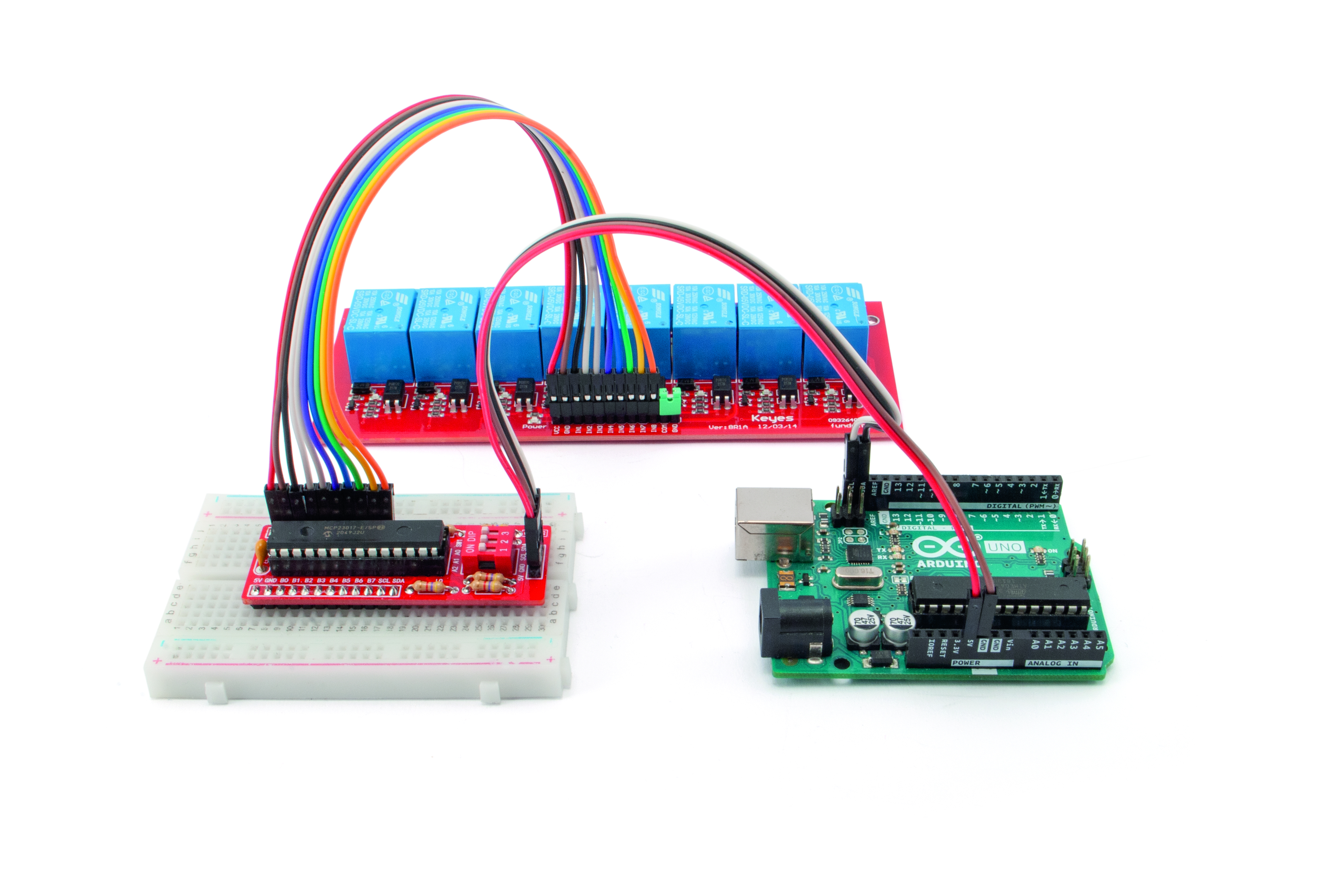
The breakout board was created to be interfaced to a microcontroller, since typically, I/O-expanders are used by devices equipped with a serial interface to I²C Bus; since Arduino supports this bus, download the sample code for MCP23017's I/O so that you can write it to your board via the IDE. This sketch basically allows you to write the state of the Port A register as a function of a byte sent by Arduino along the bus, whose bits correspond to the state read on Port B, which this time acts as the input. To give the example a concrete application, we decided to use the logical states of the I/Os of Port A, which will operate here as digital outputs, to drive a relay board; specifically, we need to connect the 8 relay output control lines of the RELAY8CH board to the I/O bank of Port A, while 8 normally open pushbuttons are to be connected to Port B, having in common the pole connected to GND. To realize this application, it is necessary to connect Arduino UNO, the breakout board, the relay board and the buttons, as shown in the wiring diagram proposed in Figure 3, whilst Figure 4 shows the real prototype of this application. Since these are quite common pushbuttons (normally open) and have no external electronics, the internal pull-ups of the MCP were enabled (via library) to handle them and recognize the change of state, so we activated the respective output when the button is brought to ground (GND). To accomplish this, a simple Arduino UNO-based code was written, taking advantage of the Adafruit library, which, as you see in Listing 1, is included in the first line of the sketch that follows:
#include <Adafruit_MCP23X17.h>
Adafruit_MCP23X17 mcp;
int i = 0;
int OUT[] = {7,6,5,4,3,2,1,0}; //Represents MCP23017 PIN (A7...A0)
int IN[] = {8,9,10,11,12,13,14,15}; //Represents MCP23017 PIN (B0...B7)
int STATO[] = {0,0,0,0,0,0,0,0}; ◦ //For each output, every toggle the status is being saved
void setup()
{
Serial.begin(9600);
Serial.println("MCP23017 INPUT/OUTPUT");
if (!mcp.begin_I2C(0x20)) //0x20 is MCP23017's address with A0=A1=A2 > ON(GND)
{
Serial.println("MCP Error!"); //If MCP is not found, the error is visualized
while (1);
}
//bank A Pin set as outputs and B bank as inputs
//The STATO variable to 0 to indicate idling outputs
for (i=0; i<8; i=i+1)
{
mcp.pinMode(OUT[i], OUTPUT);
mcp.pinMode(IN[i], INPUT_PULLUP);
STATO[i] = 0;
}
}
//******************* L O O P **********************
void loop()
{
String Testo_Debug = "";
for (i=0; i<8; i=i+1)
{
//If button pressed or output not activated, I activate it
if ((mcp.digitalRead(IN[i])==0) && (STATO[i]==0))
{
STATO[i] = 1;
Testo_Debug = "Pulsante" + String(i+1) + "premuto";
Serial.println(Testo_Debug);
mcp.digitalWrite(OUT[i], HIGH);
}
//If button released and output is active, I deactivate it
if ((mcp.digitalRead(IN[i])==1) && (STATO[i]==1))
{
STATO[i] = 0;
Testo_Debug = "Pulsante" + String(i+1) + "rilasciato";
Serial.println(Testo_Debug);
mcp.digitalWrite(OUT[i], LOW);
}
}
delay(10);
}
Before loading the code into the program memory of our Arduino board, it is essential to download the library from Adafruit and install it using the Library Manager included in the IDE, or simply extract the contents of the ZIP file and then copy the entire Adafruit_MCP23017_Arduino_Library folder within the libraries directory normally found within the operating system at the path Documents\Arduino\libraries. Having loaded the library, it will be sufficient to load our example code and load it inside the board after choosing the correct COM port from the Tools menu of the IDE.
In the code, a byte is requested to be sent to the MCP23017, containing the status of the buttons, and the related data is processed and then written to a byte directed to the integrated, which will set the status of the Port A lines in a stable manner, until the refresh. For the interfacing to work, dip-switches A0, A1 and A2 must be set correctly because if the sensor was not assigned the address 0x20, an error message would be shown on the serial; the breakout board address is assigned with the 000 combination of the three bits A0, A1, A2, i.e.,closing all three dip-switches to ground. If you want to change the address, refer to the usual Table 1, with the understanding that you must change the address written in the sketch.
Component List
- Resistors: R1 to R6: 4.7 kΩ
- Capacitor: C1 100 nF, ceramic
- Semiconductor: U1 MCP23017-E/SP
- Various: SW1 3-Way Dip-Switch; 14 + 14 Pin DIL socket; 2 × 12 Pin Header, male; 1 × 4 Pin Header, male; 1 × PCB (see text)
Editor's note: This project originally appeared in Elettronica IN.
Discussion (1 comment)